Tutorial
MaKING Printed Circuit Boards with Wild Clay
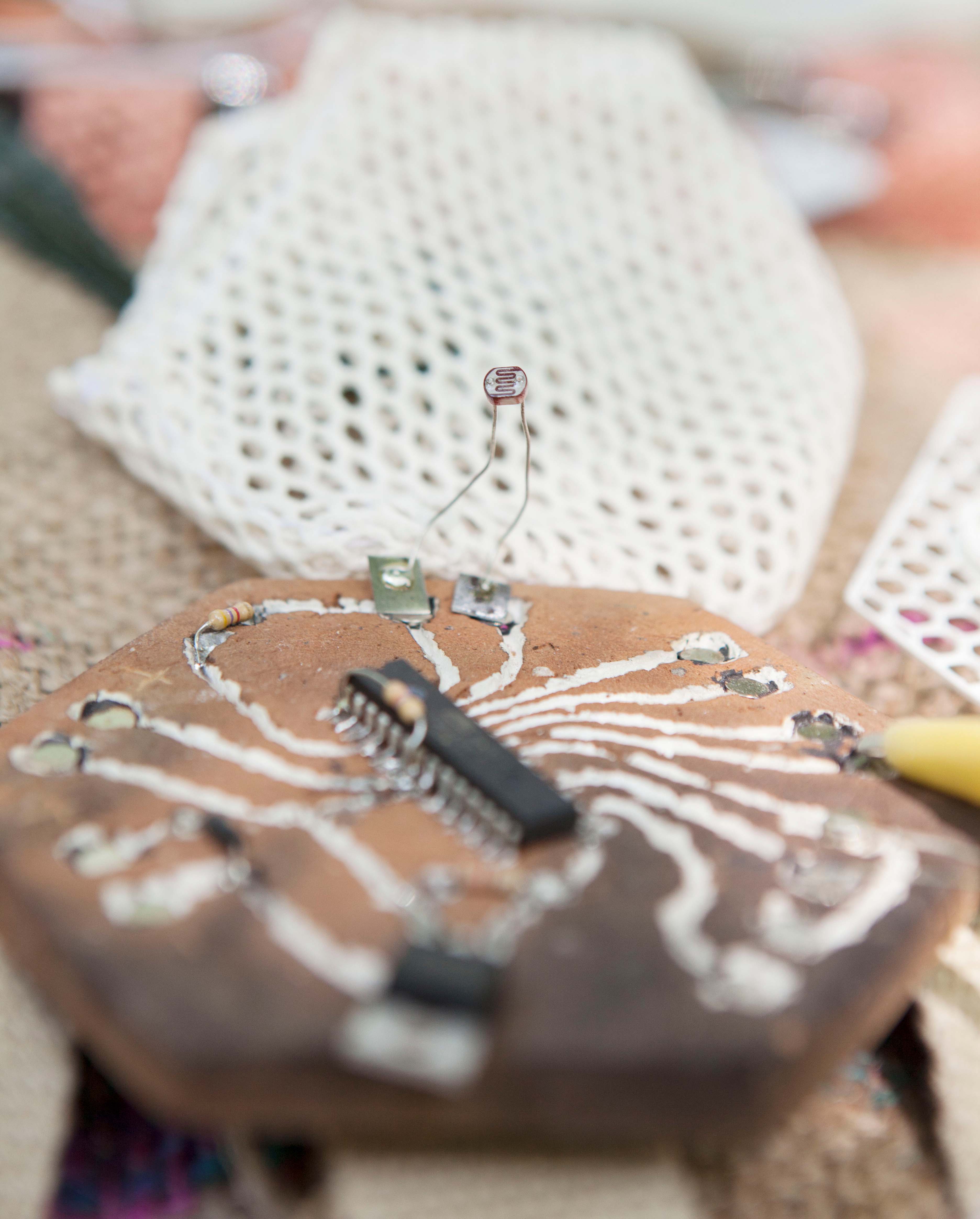
It is an open secret that the hardware in our smart devices contains not only plastics
but also conflict minerals such as tungsten, tin, tantalum, silver and gold.
We are
investigating alternative hardware from locally sourced materials, so-called ethical
hardware, to develop and speculate upon renewable practices for the benefit of both
nature and humans.
We are exploring different materials, sentient, low-impact, non-toxic, fair traded,
recycled and urban mined means of production.
We aim to challenge the common PCB
(printed circuit board) economies in an artistic, creative, positive and responsible way
applying feminist hacking as an artistic methodology and critical framework.
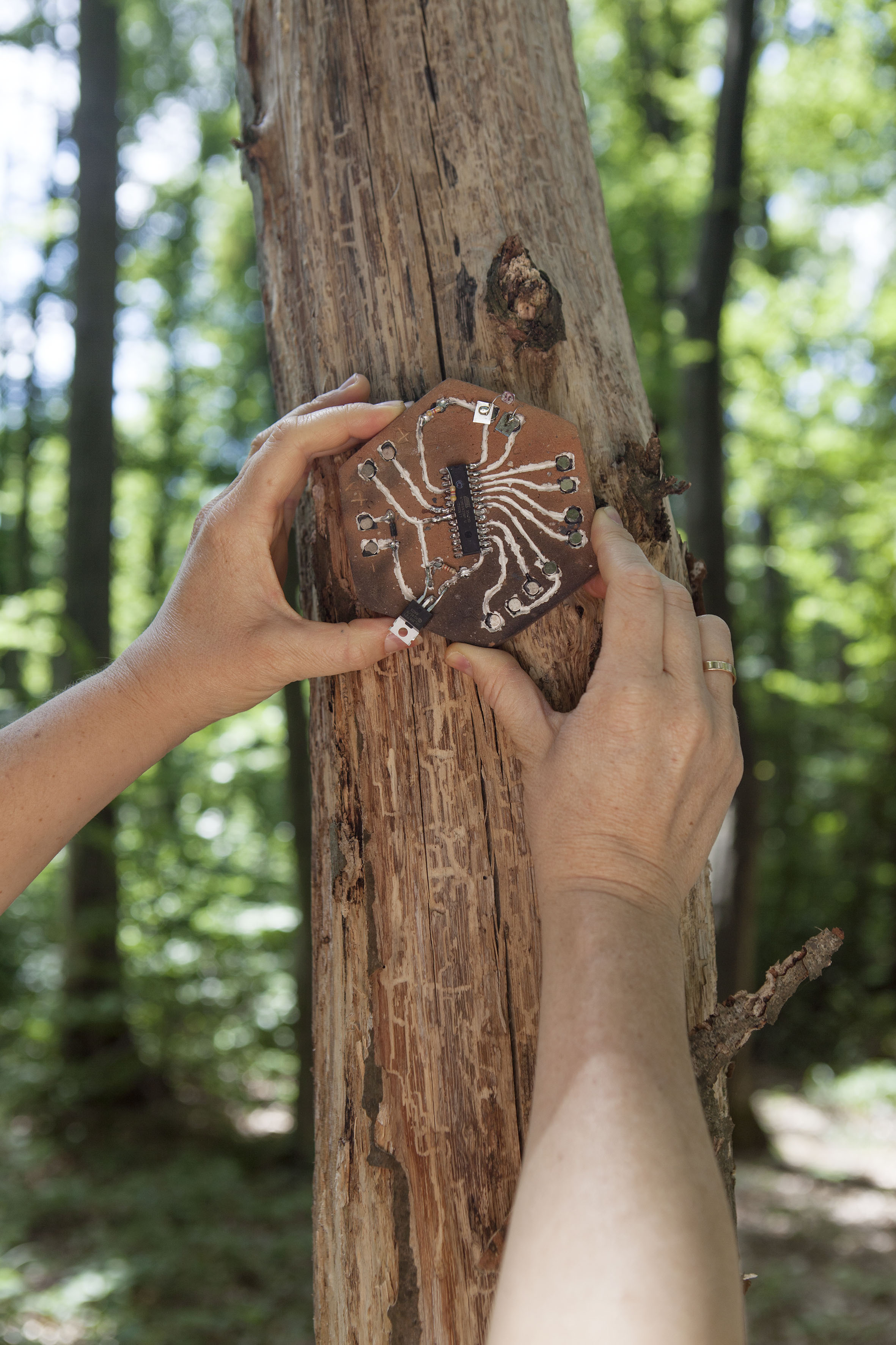
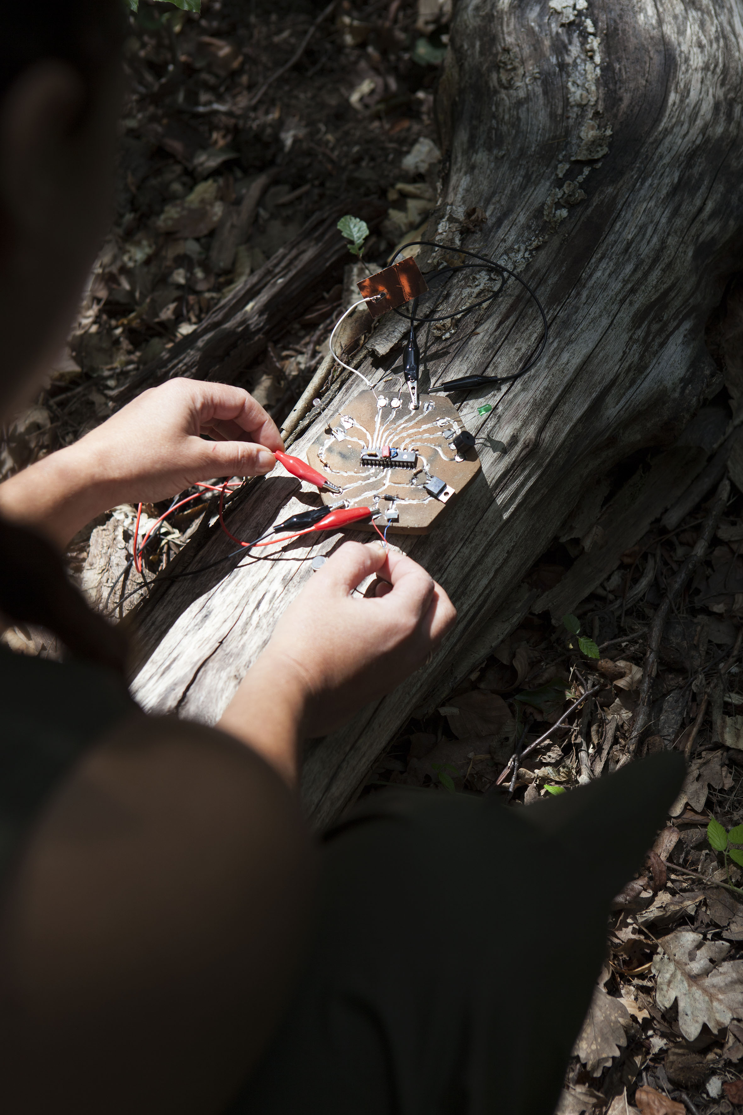
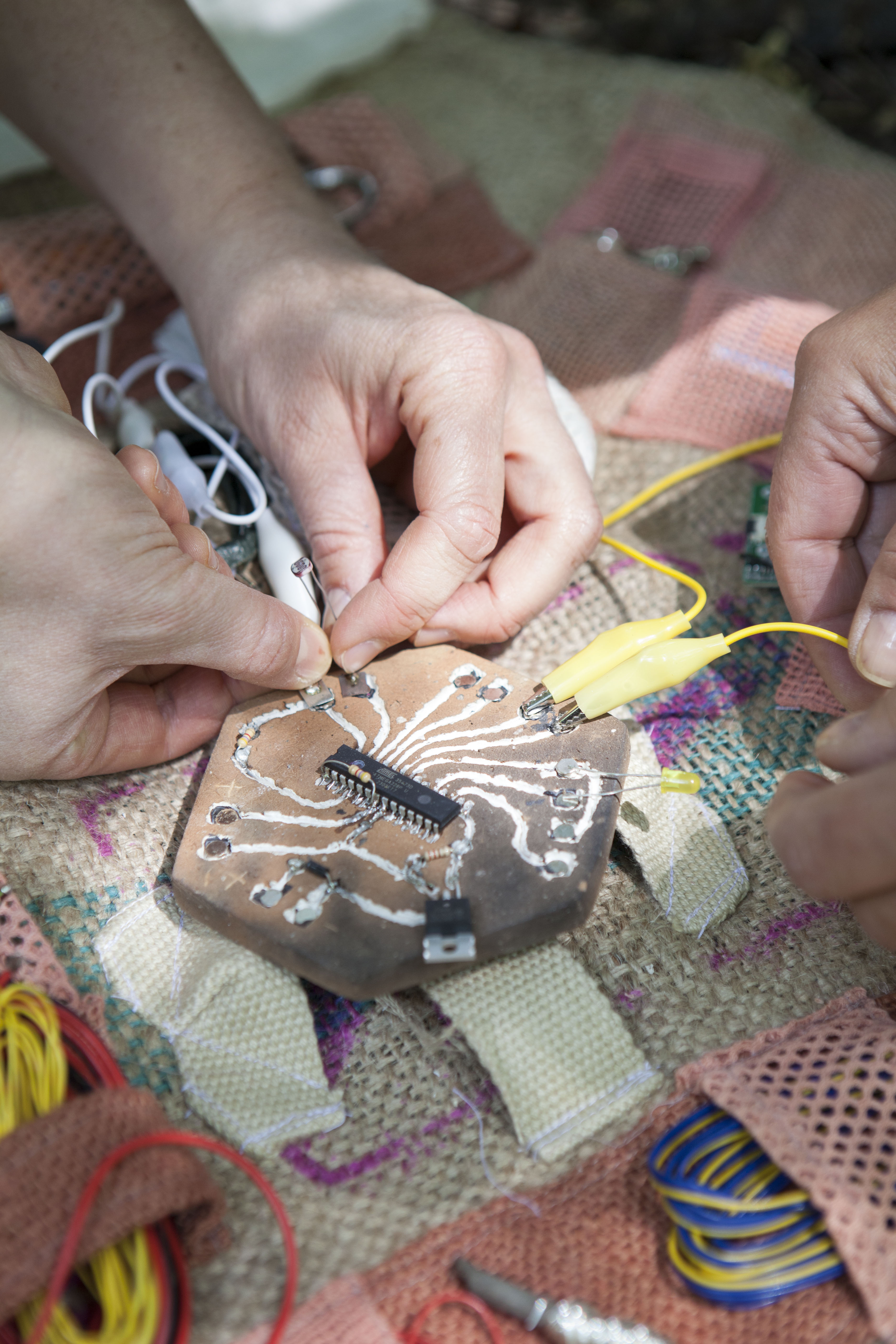
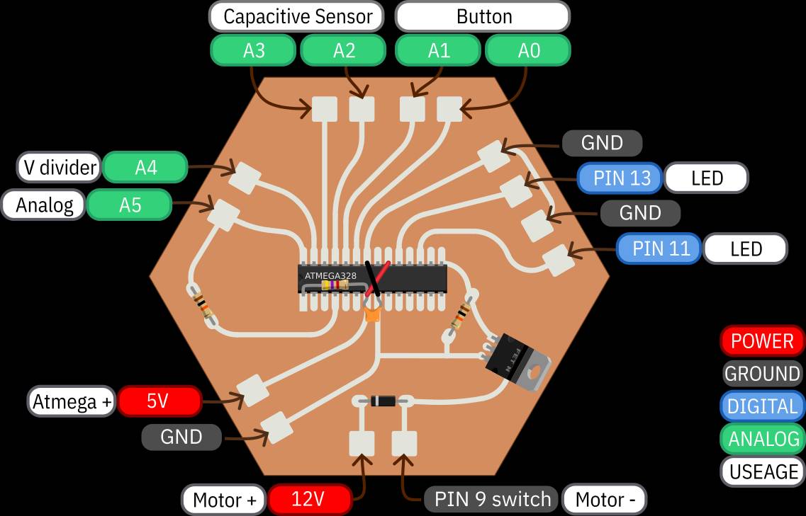
Our initial idea was to develop a microcontroller PCB that could work with the
ATmega328P chip, which is commonly used in the famous Arduino Uno board (orArduina board, as some feminists call it). Why this chip? Because we are part of a
community hackerspace –
— Mz* Baltazar’s Lab (a feminist hacklab and artist-run independent space based in Vienna, Austria) – and the Arduino Uno has been our favourite microcontroller for the past 12 years. After using it in many prototypes, artworks and workshops, we had several malfunctioning Arduino boards left over. But their chips were still working, so the idea was to reuse the chips in our new project.
The second challenge was to come up with an electric circuit that would allow us to receive several forms of input signal (analogue and digital sensors) and generate a variety of output signals (to control LEDs, motors and speakers).
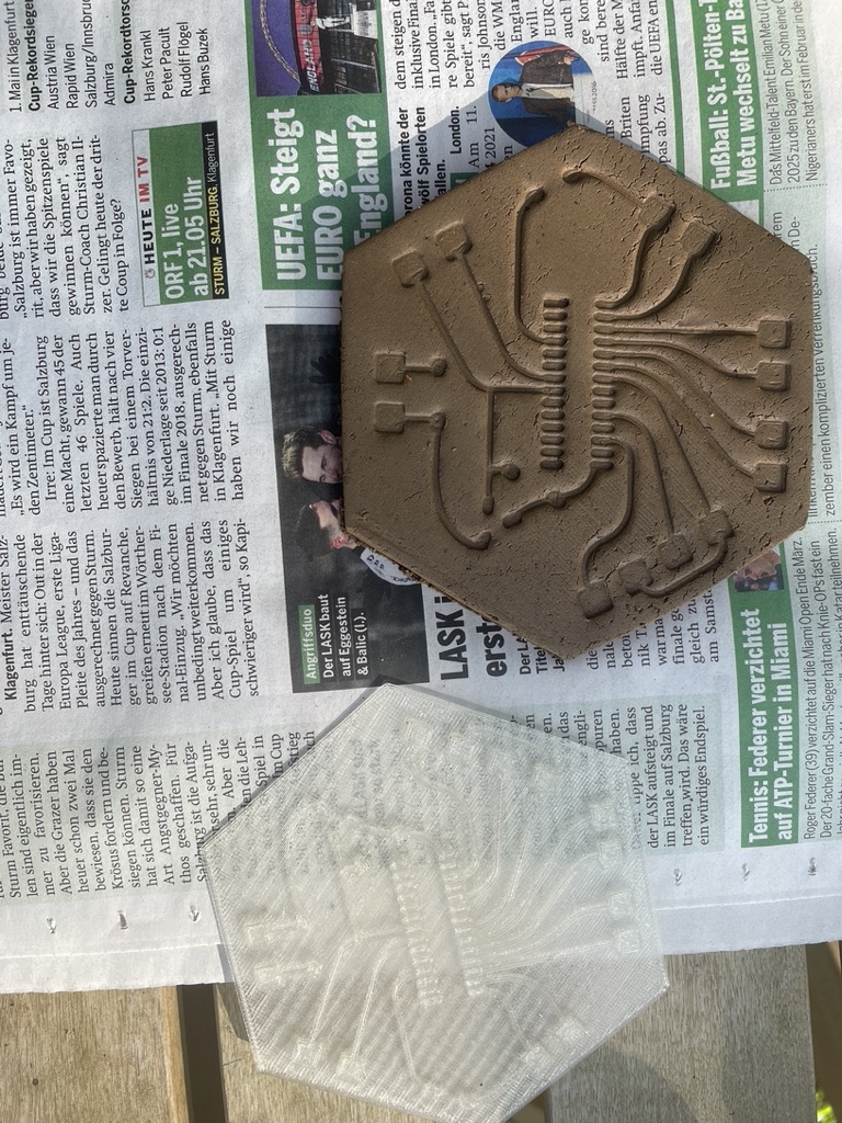
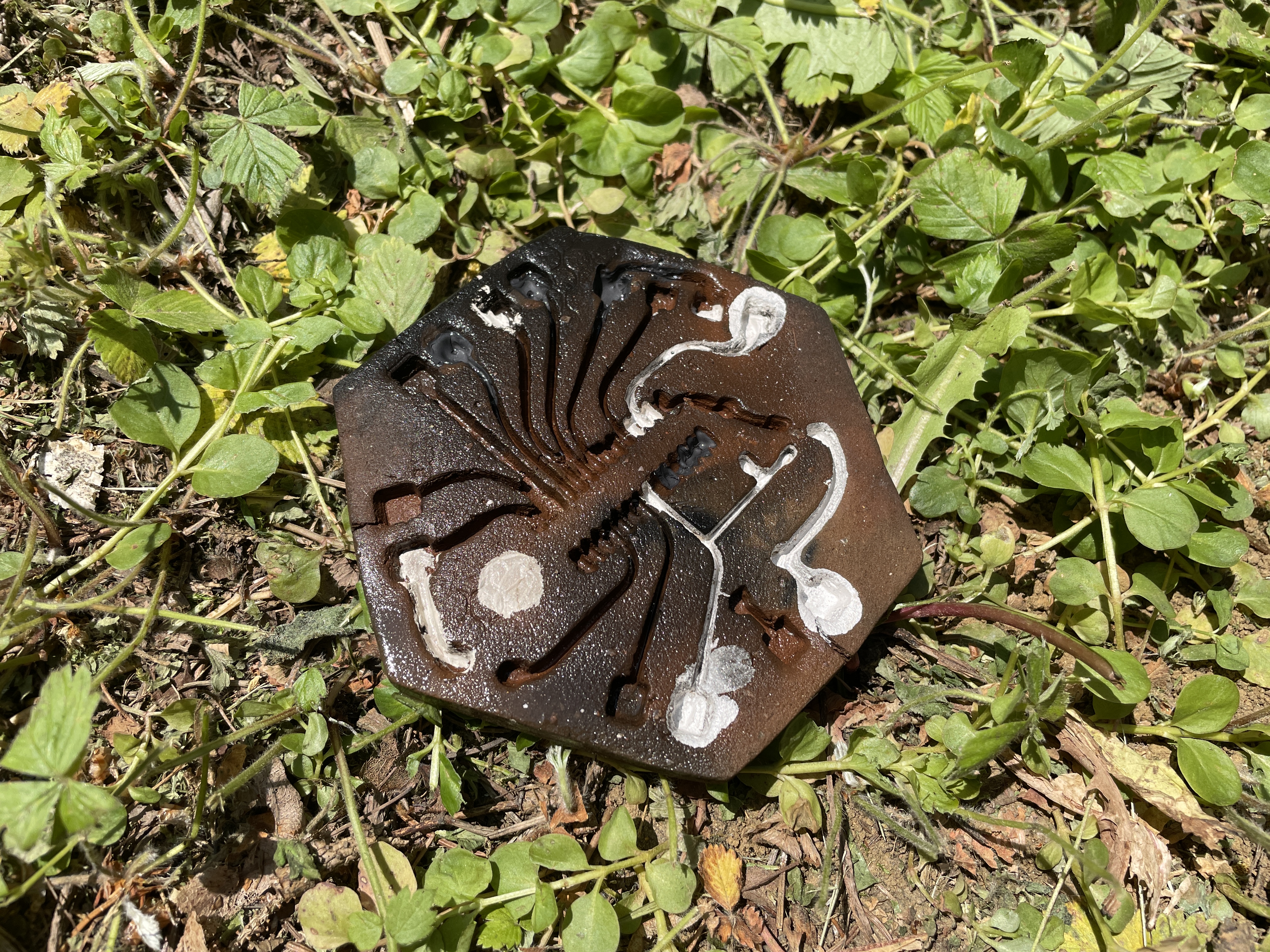
With this insight, we were able to design a 3D printed !stamp‘ using a recycled
polypropylene filament. This process took a while, because we had to consider the
clay’s changed size after drying and firing. All clay shrinks considerably during the
drying and firing process. We estimate that there is a 5% shrinking rate, but this
might vary depending on the clay you are working with. We also experimented with the
depth of the circuit tracks and realised that the imprint should ideally be 1.2 mm
deep.
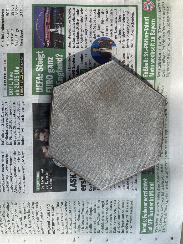
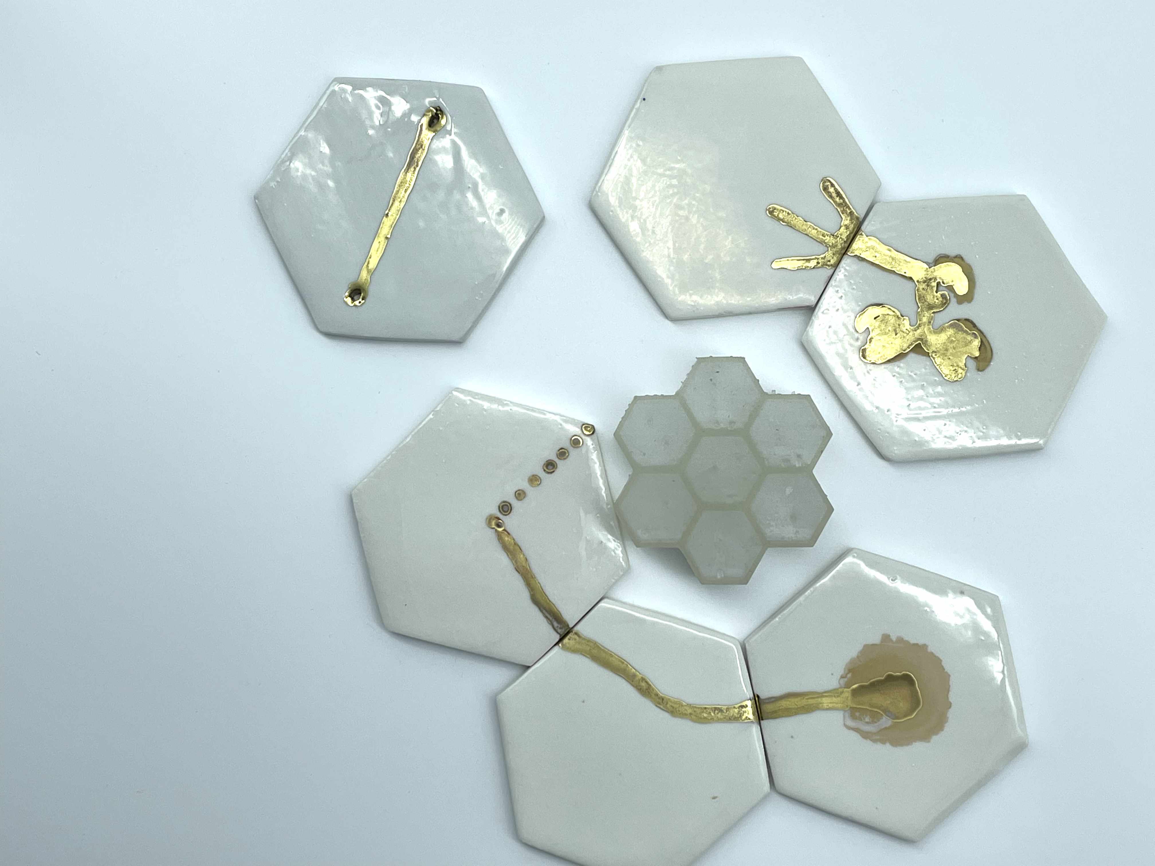

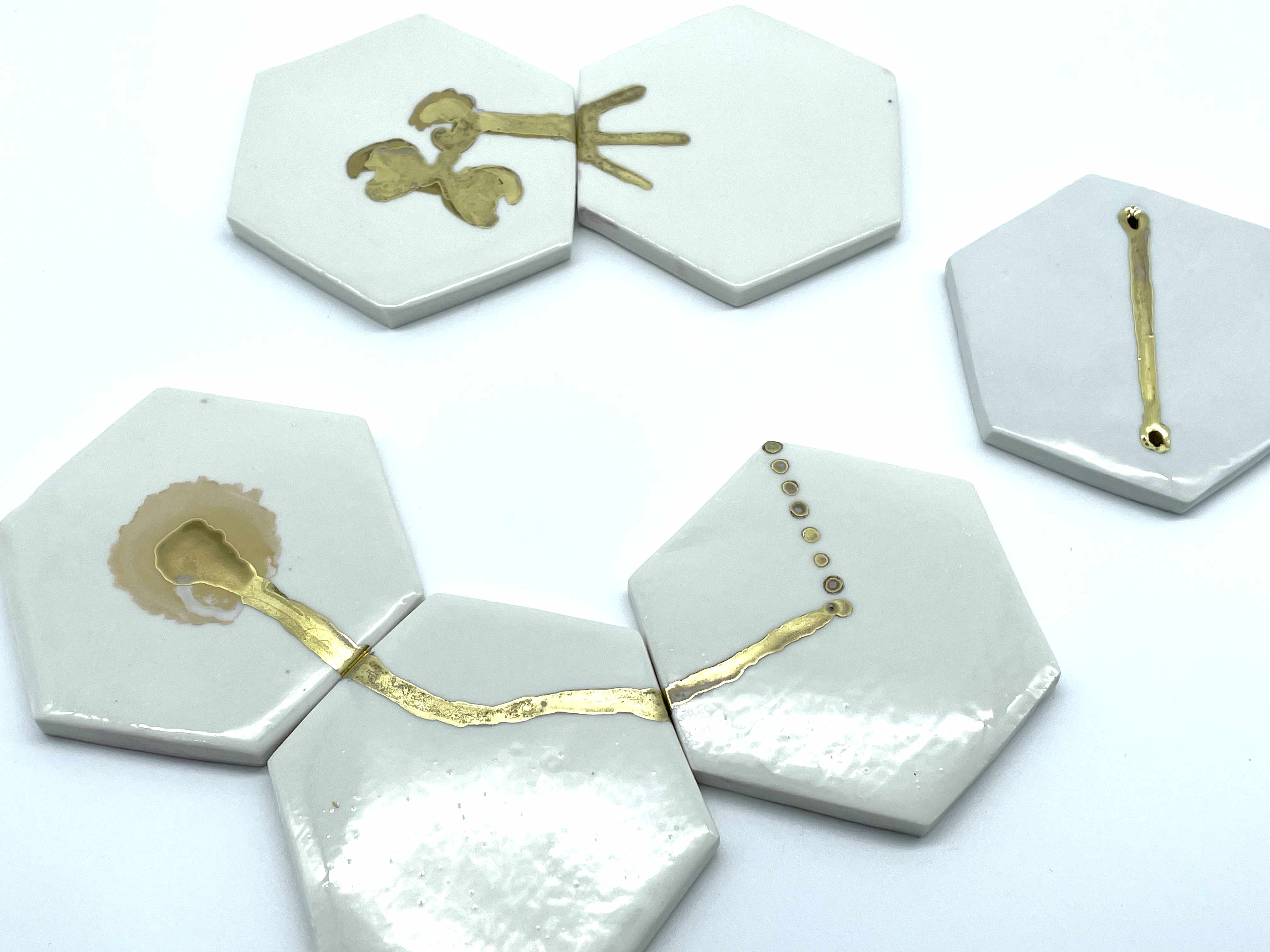
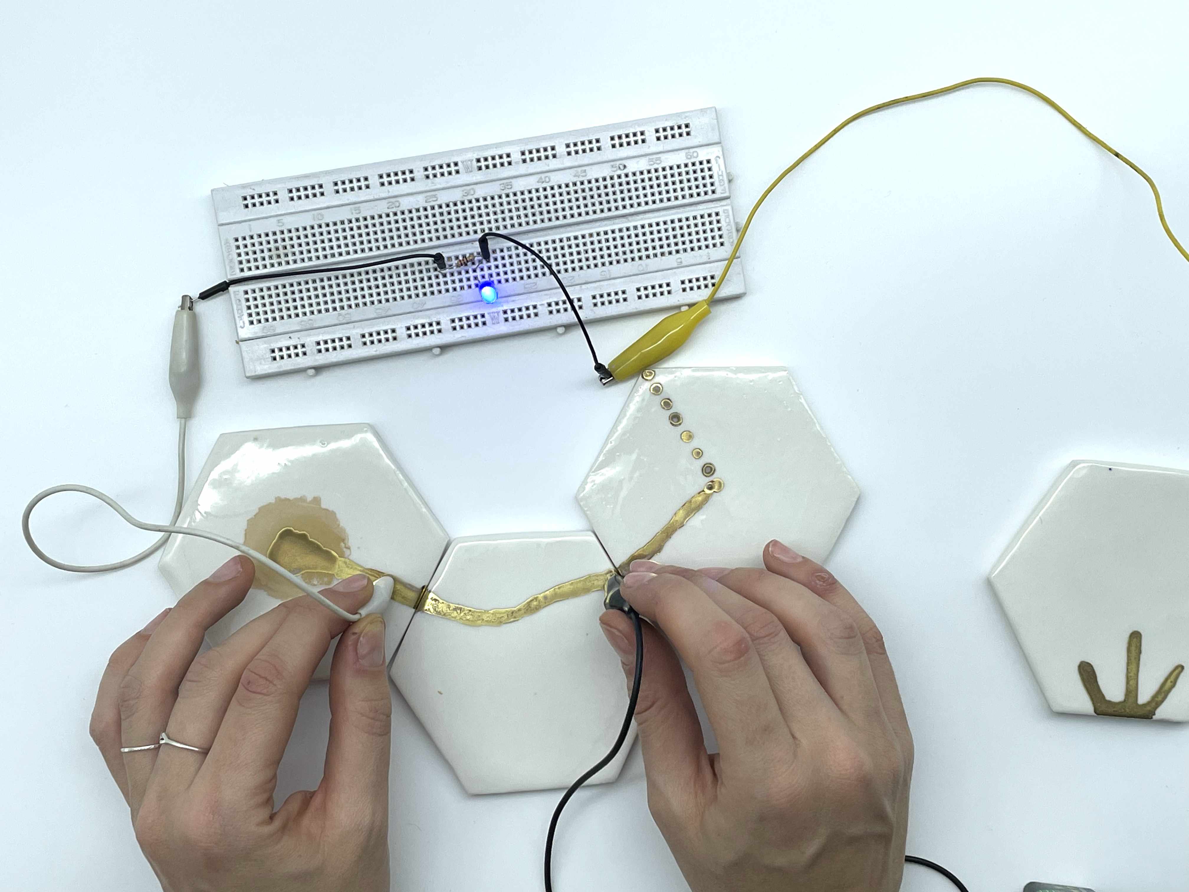

To build the base of our PCB, we needed insulating, sustainable and robust materials
(eggshells? wood plates? wax? ceramics?). We immediately chose ceramics, specificallyporcelain, as it already plays an important role in electronic components such as
capacitors, piezo, resistors, and so on. Porcelain is an industrially made material
comprising kaolin (the main ingredient that makes it plastic and white) and stone
pottery (the second ingredient that makes porcelain translucent and hard). Both are
well-known commodities that are prospected and mined around the world, on a small
scale in Europe and a larger scale in China, Brazil, South Africa and Vietnam (among
others).
In pottery, porcelain, also known as china clay, is a very delicate and sensitive material (we could say it has its own agency), more difficult to control than other industrial clays. Also, along with the other harder and more resistant stoneware clays, it usually requires higher firing temperatures, in two stages: a first firing known as a ceramic bisque of c. 1000 oC; and a glazing firing around 1200 oC in an electric kiln. During our initial experiments with porcelain, we were immediately aware that the higher temperatures, and therefore electric consumption, were not compatible with our standards for ethical hardware.
In pottery, porcelain, also known as china clay, is a very delicate and sensitive material (we could say it has its own agency), more difficult to control than other industrial clays. Also, along with the other harder and more resistant stoneware clays, it usually requires higher firing temperatures, in two stages: a first firing known as a ceramic bisque of c. 1000 oC; and a glazing firing around 1200 oC in an electric kiln. During our initial experiments with porcelain, we were immediately aware that the higher temperatures, and therefore electric consumption, were not compatible with our standards for ethical hardware.
It was when we were struggling with the question of how to manufacture clay in low-energy and low-impact ways that we came across the work of Heinz Lackinger, a
pottery crafter in Donnerskirchen, Burgenland, Austria, who works with prehistoric
techniques of firing clay in an open wood fire. Instead of using sophisticated machines,
he uses a simple hole in the grounds of his 18th-century house. We had the privilege of
spending two days with this skilled craftsman, learning how to identify and collect the
clay, and how to model and fire it using old, dry branches collected from the forest
ground. If the clay is collected with awareness of its many qualities, and in small
quantities only, this process can be defined as 100% fair trade and congruent with
locally sourced modes of hardware production. We owe the knowledge required for the
following steps to Heinz Lackinger’s generous knowledge transfer during his
workshop, and to our own experiments later applying this technique in the making of
natural clay PCB boards.
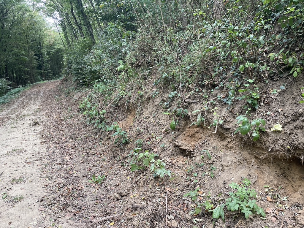
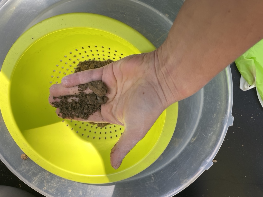
We collected our clay at the beginning of autumn in dry weather. The soil is mainly dry
at this time, but it doesn’t consist of argil alone: you will find small stones, plants, even
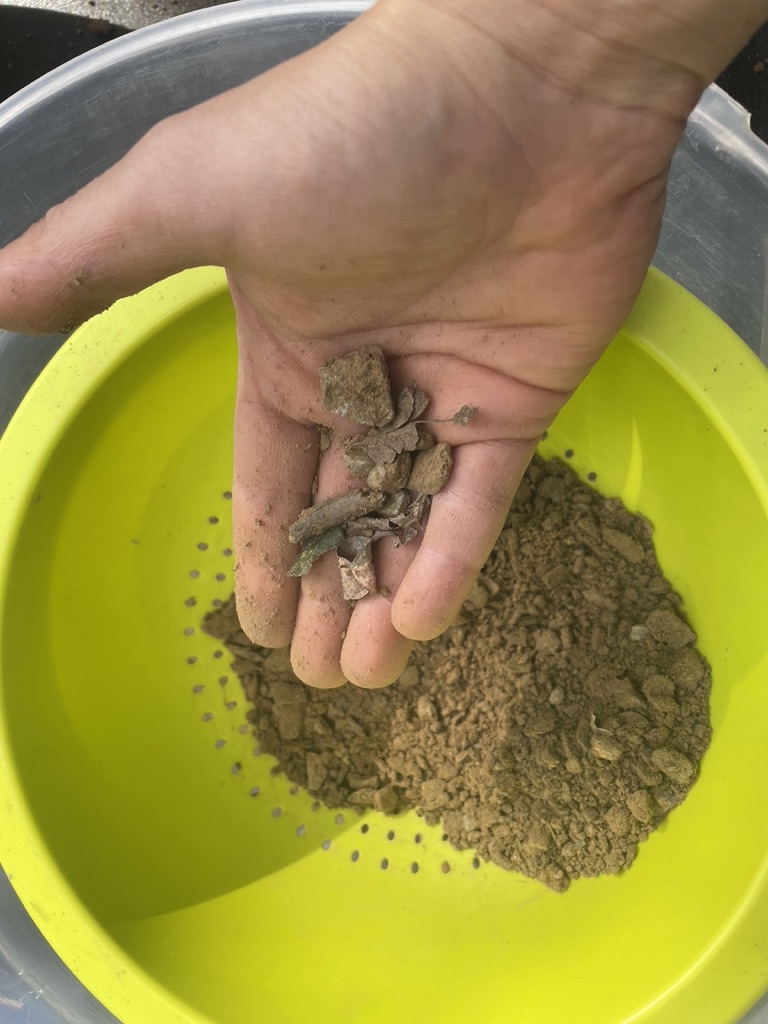
small insects. When the clay is that dry, the easiest way to clean it is using a net that
retains the undesirable waste. Our favourite tool for this is a standard kitchen
colander. The waste collected should be given back to the earth, put back in the
ground.
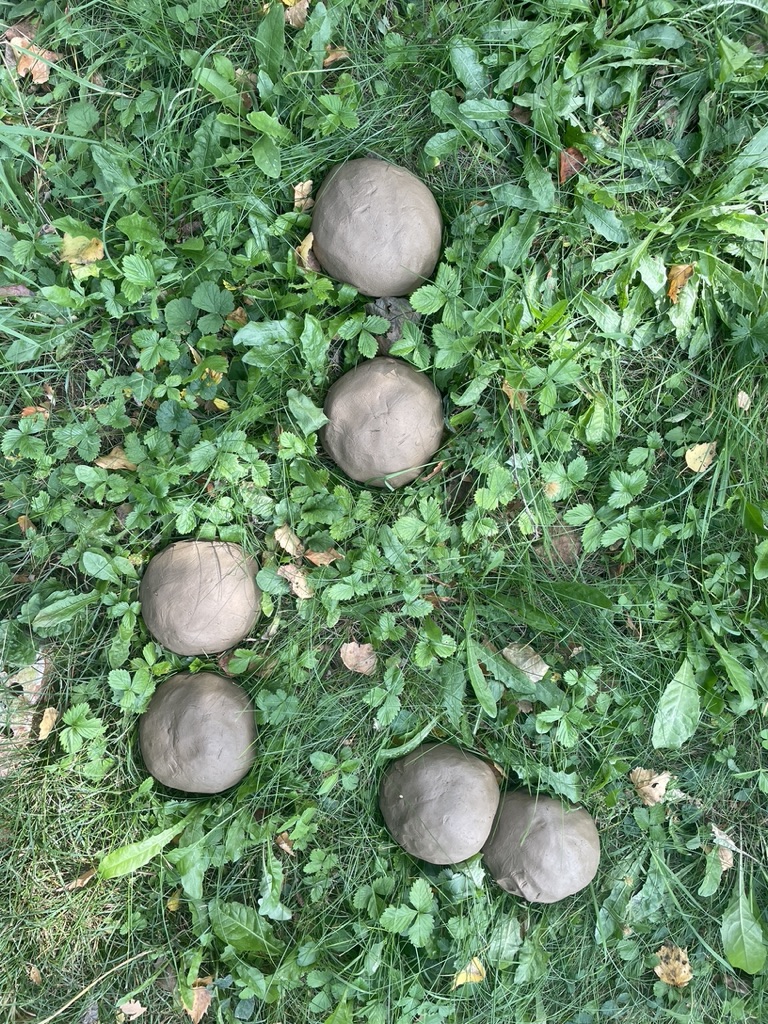
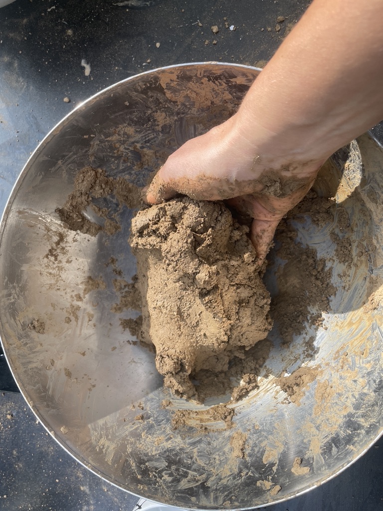
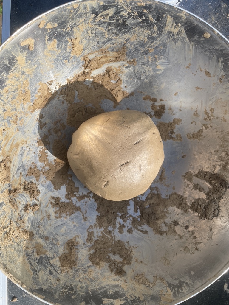
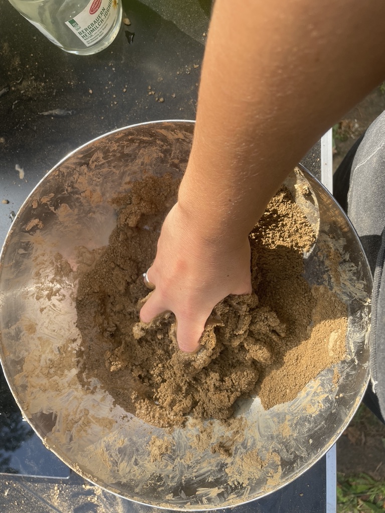
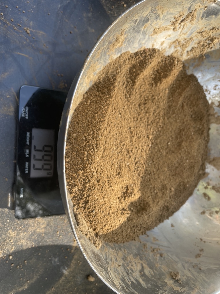
You will end up with a fine powder that needs some water. We calculated an average of100 ml of water per 1 kg of fine powder. Mixing it is just like blending flour and water, but without the inconvenient grumps. You should end up with something like a ball of clay after 10 minutes of massaging. It is important that the clay sticks together and all the air is removed.
You will end up with a fine powder that needs some water. We calculated an average of100 ml of water per 1 kg of fine powder. Mixing it is just like blending flour and water, but without the inconvenient grumps. You should end up with something like a ball of clay after 10 minutes of massaging. It is important that the clay sticks together and all the air is removed.
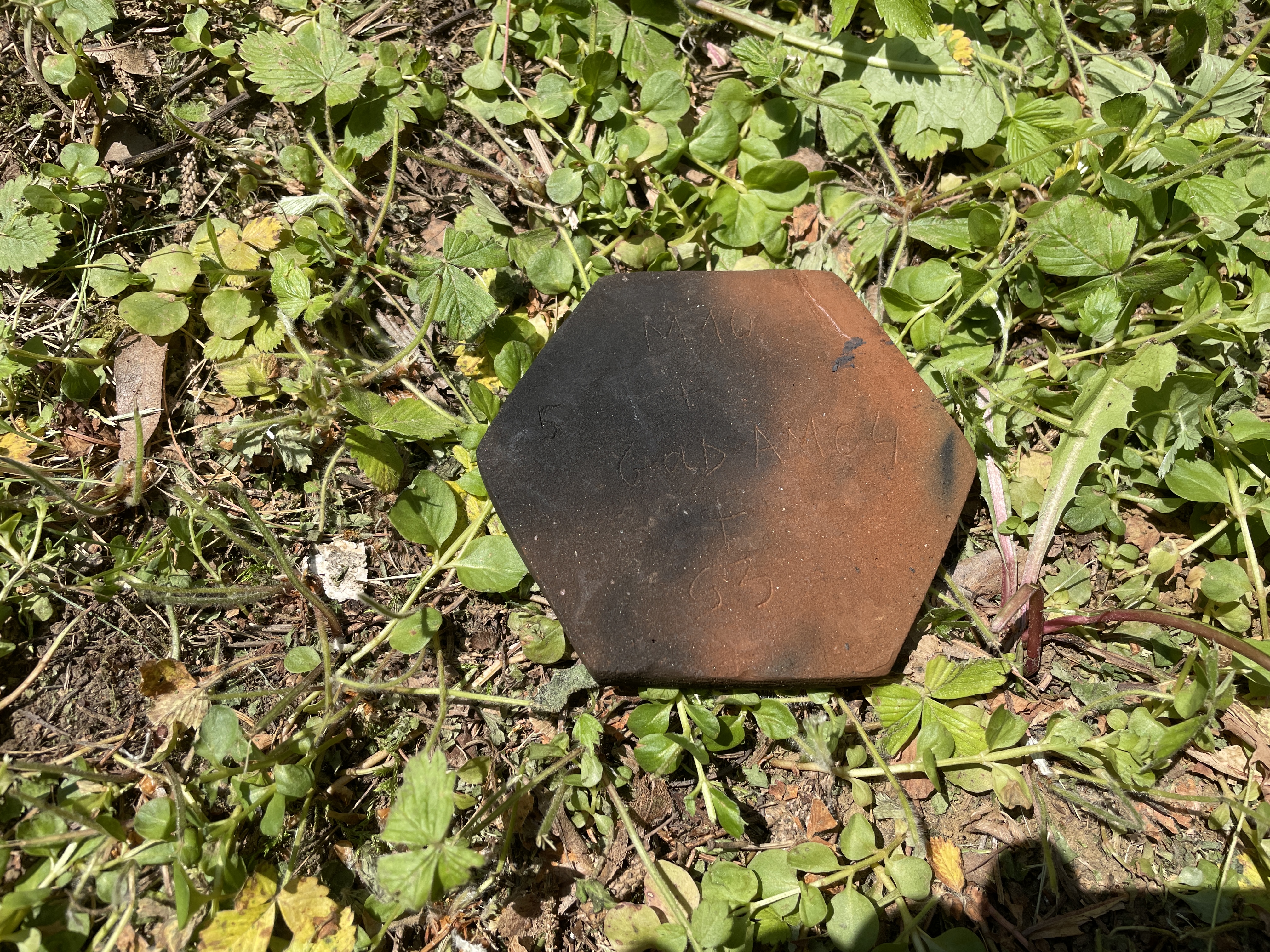
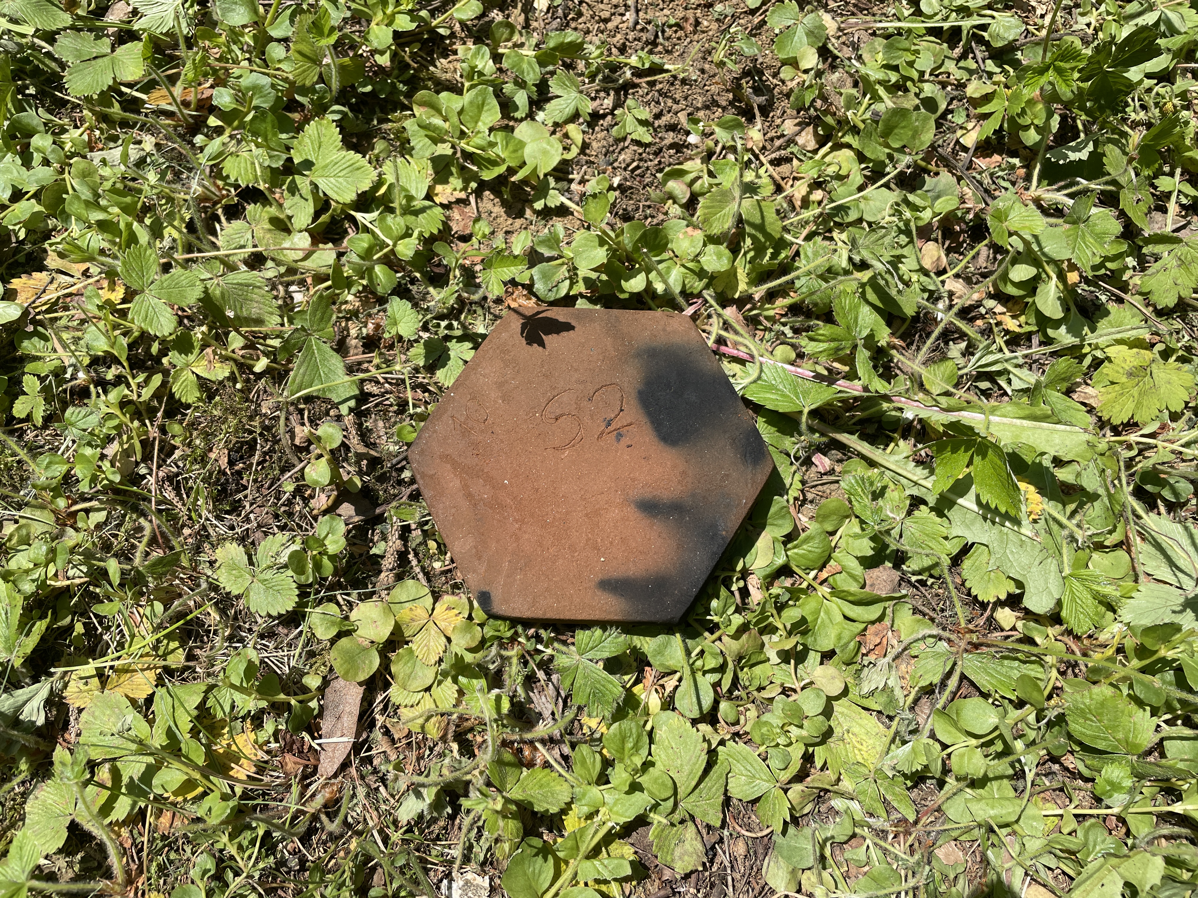
For the shape of our PCB board, we used a hexagon tile cutter measuring 10 x 10
cm, which can be bought in most ceramic shops. We chose a hexagon shape, as the tile
form is not mandatory; but you can pick any shape and thickness you desire, as long
as it maintains a printable surface of c. 10 x 10 cm. We chose this shape and format in
the hope of assembling the boards as tiles next to one another, connecting them
electronically. We ultimately abandoned this idea, since it was very difficult with this
material to obtain straight edges that exactly lined up.
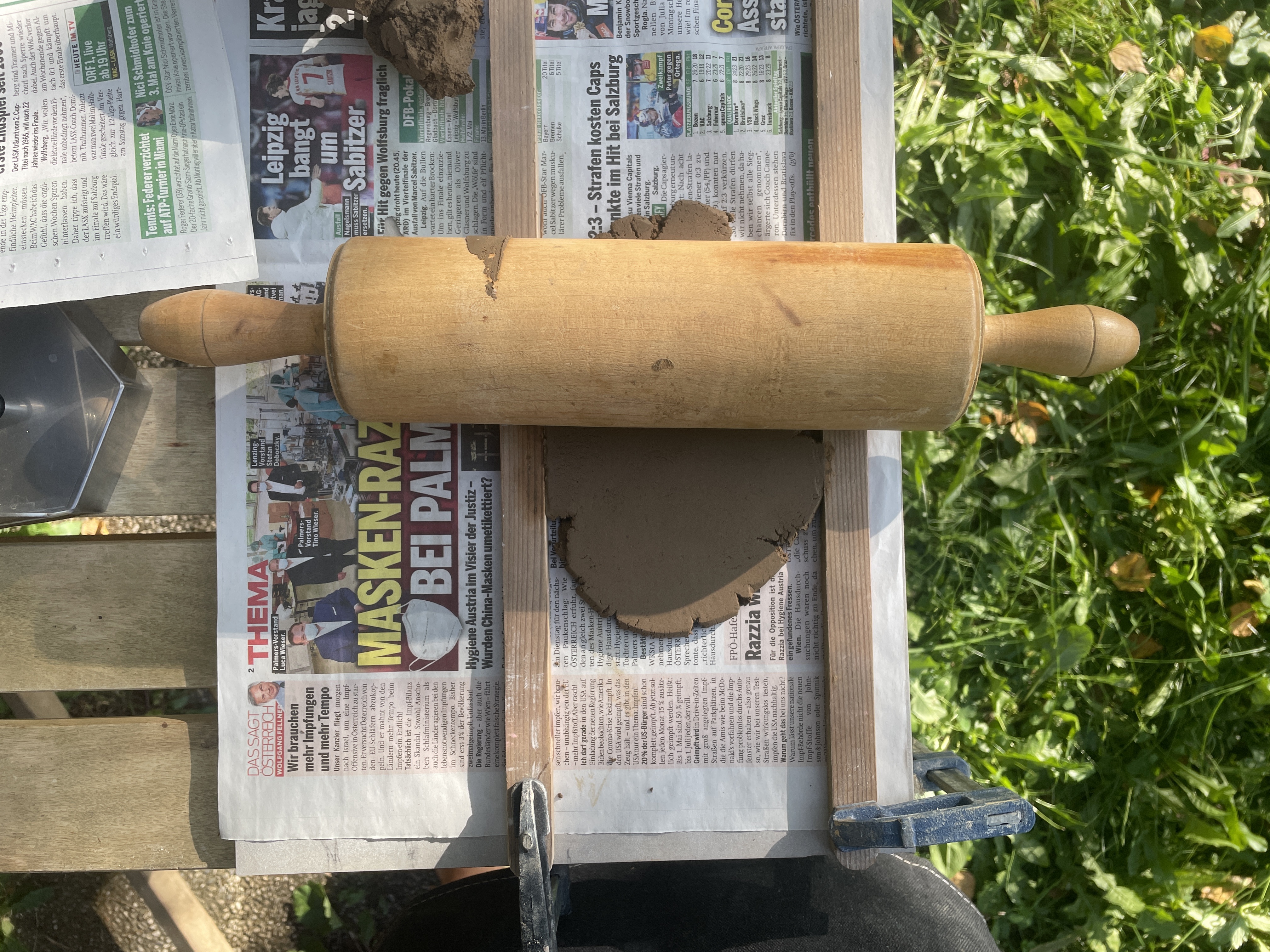
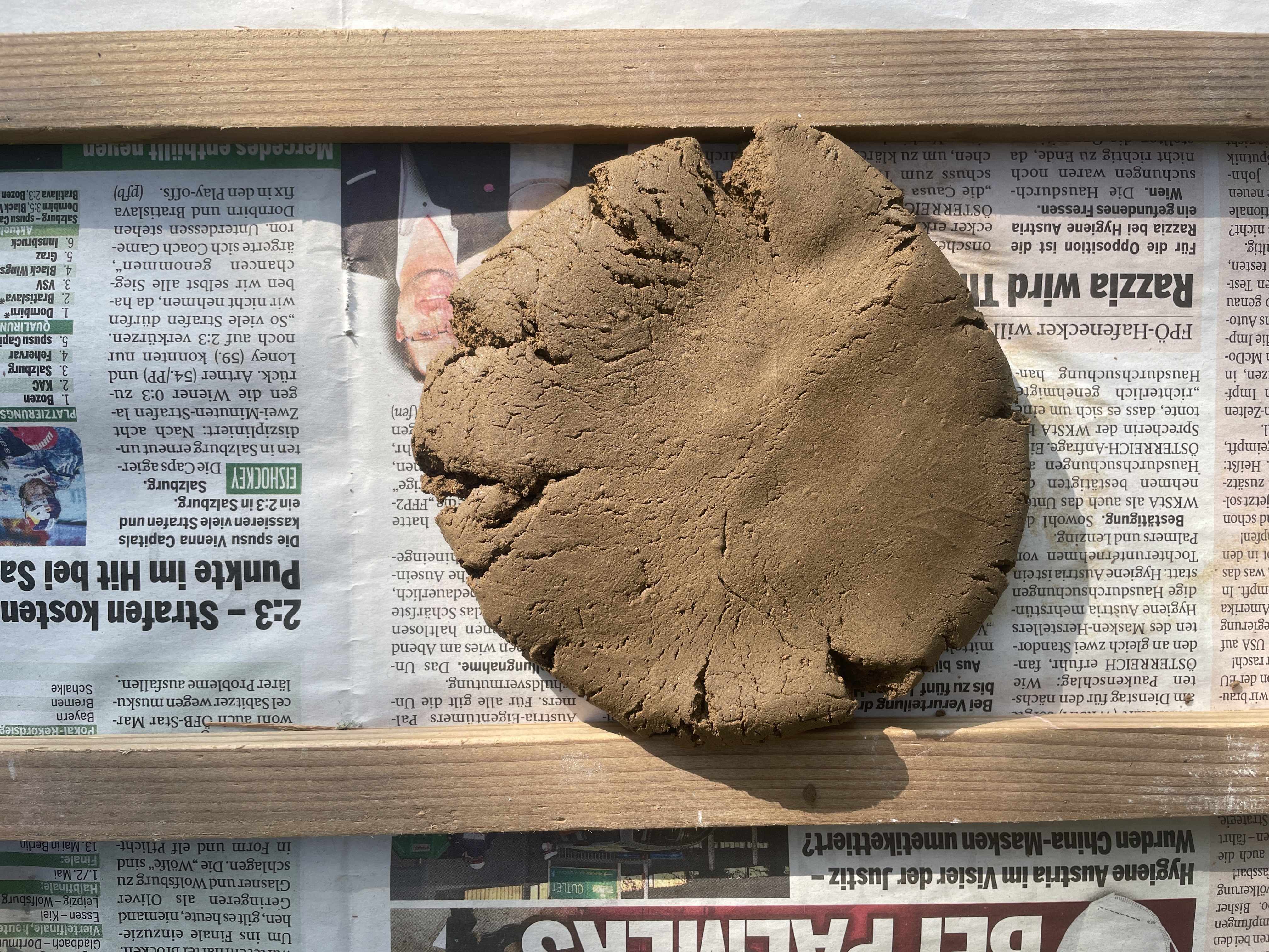
To facilitate the process, we used two small wooden slats of 1 cm thickness, which we attached with clamps to a table. The distance between the slats was c. 10 cm. We also used a newspaper sheet underneath to avoid the clay sticking to the surface of the table (a plaster surface works best of all). Before placing the clay between the slats, it is important to prepare it in small quantities. Each board requires around 180 g so we recommend taking something around 220 g and kneading it thoroughly for a minute to get rid of any air bubbles, shaping it into a ball. (If your clay is not even enough, it is better to throw it down forcefully against a flat surface and repeat the process a couple of times.) When you"re ready, place it between the slats and gently press it, bearing down on it until it is flat enough for the area you want to achieve. We used a dough roller to flatten out the clay to 1 cm thickness.
To facilitate the process, we used two small wooden slats of 1 cm thickness, which we attached with clamps to a table. The distance between the slats was c. 10 cm. We also used a newspaper sheet underneath to avoid the clay sticking to the surface of the table (a plaster surface works best of all). Before placing the clay between the slats, it is important to prepare it in small quantities. Each board requires around 180 g so we recommend taking something around 220 g and kneading it thoroughly for a minute to get rid of any air bubbles, shaping it into a ball. (If your clay is not even enough, it is better to throw it down forcefully against a flat surface and repeat the process a couple of times.) When you"re ready, place it between the slats and gently press it, bearing down on it until it is flat enough for the area you want to achieve. We used a dough roller to flatten out the clay to 1 cm thickness.
You will notice that the clay is very fragile and less elastic than the industrial type. It
tends to split at the edges, which is fine, as long as it is not part of your inner cutter
area.
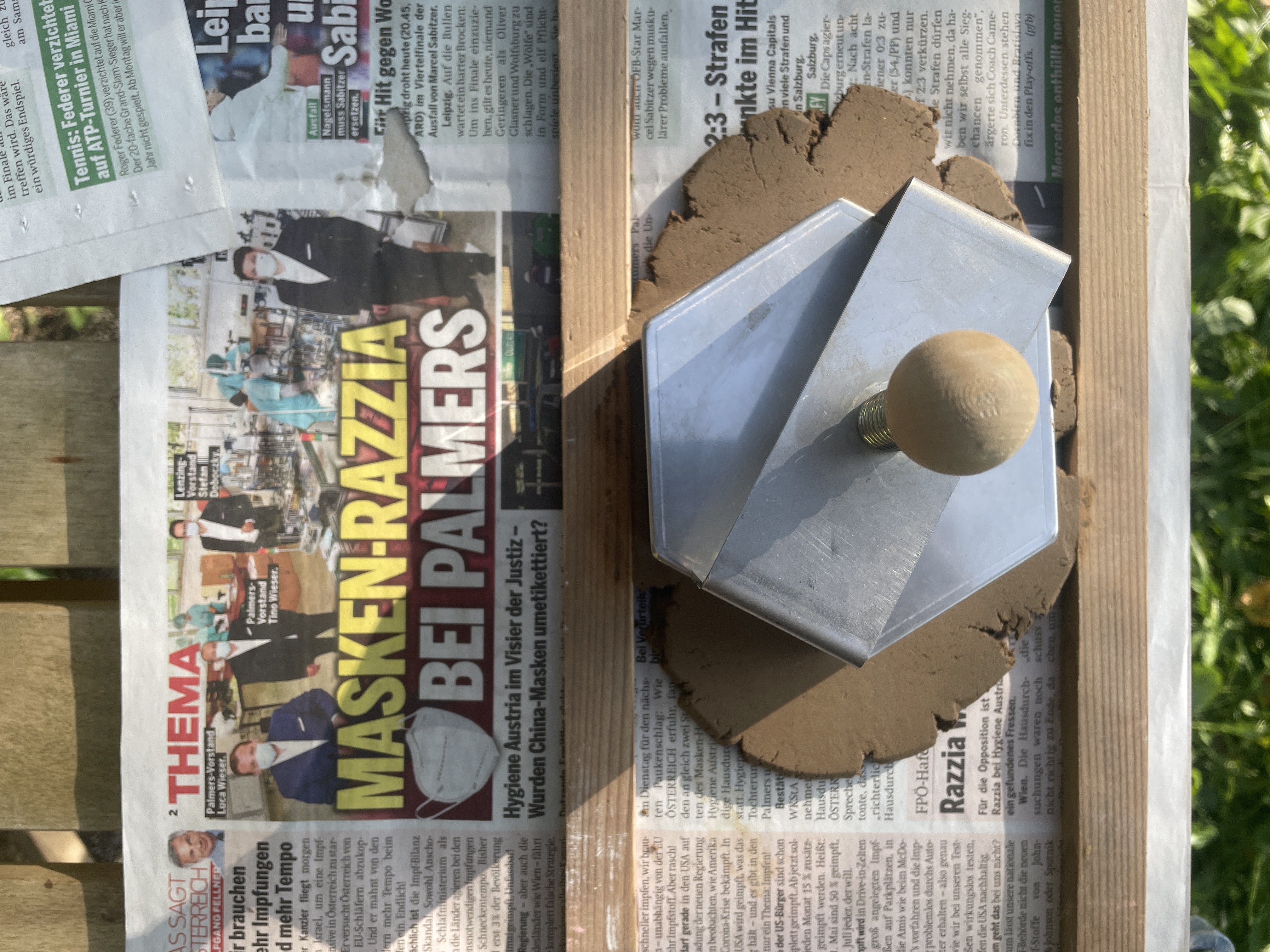
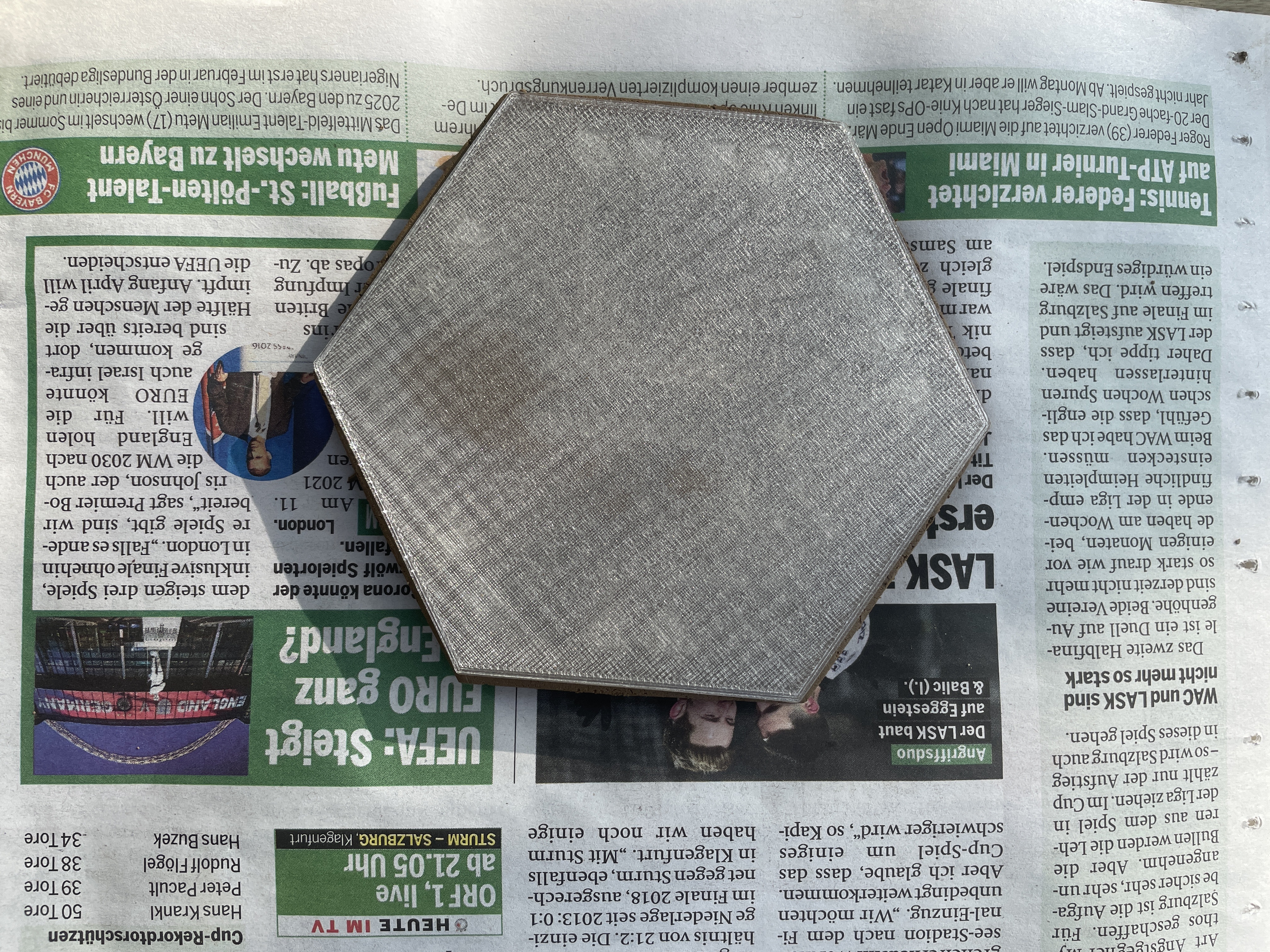
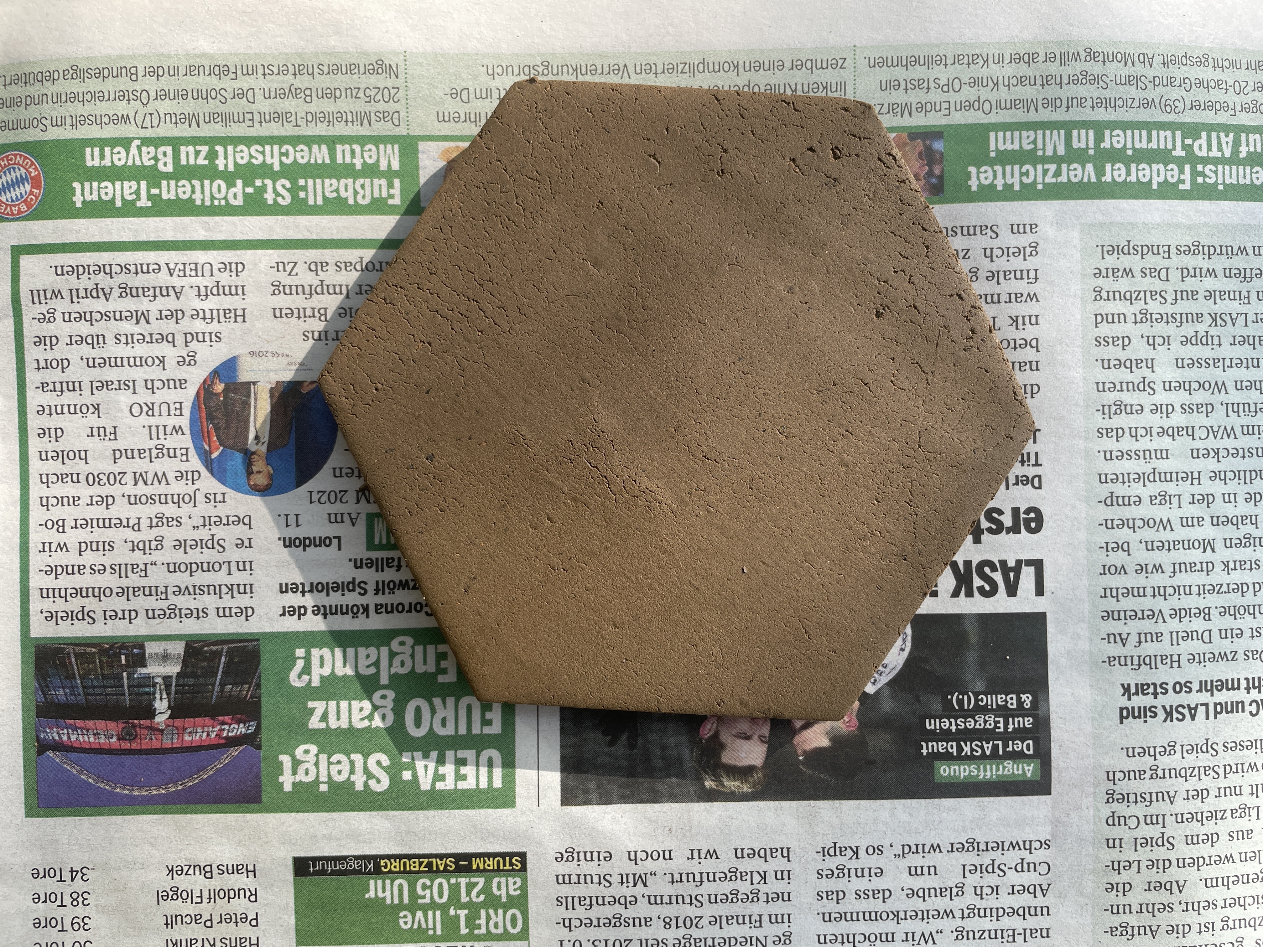
After cutting the hexagon out using the hexagon tile cutter, you can place the stamp
gently down on the clay, facing the 3D printed side down towards the clay. It is
important to apply some force, but quite gently, until the circuit is imprinted in the
clay. In this process you force the clay to deform a little at the edges, but you can
easily remove the excess material by sanding it after drying. Another technique is to
place the !stamp‘ inside the tile cutter and cut and imprint at the same time. We
observed that this also works fine. However, it is difficult to check the quality of the
imprint while pressing the cutter down. Also, the circuit tracks will be thinner, which
might make the painting process a little more difficult.
We usually let the boards dry naturally outdoors for 24 hours before painting, but this time frame is weather-dependent. If you have more time between modelling and firing the clay, you will ideally dry the boards indoors for one to two weeks, positioned between wooden plates and applying some weight to the top plate. In this way they will not deform while drying and will maintain their flat surfaces (we recommend using newspaper between the boards and the wood). If you want to dry the boards quickly, you can also place them around a wood fire. It is important to avoid temperature clashes during drying so it is best to bring them to the fire as slowly as possible, one step at a time.
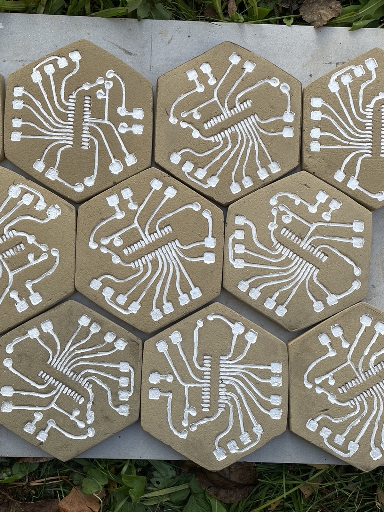
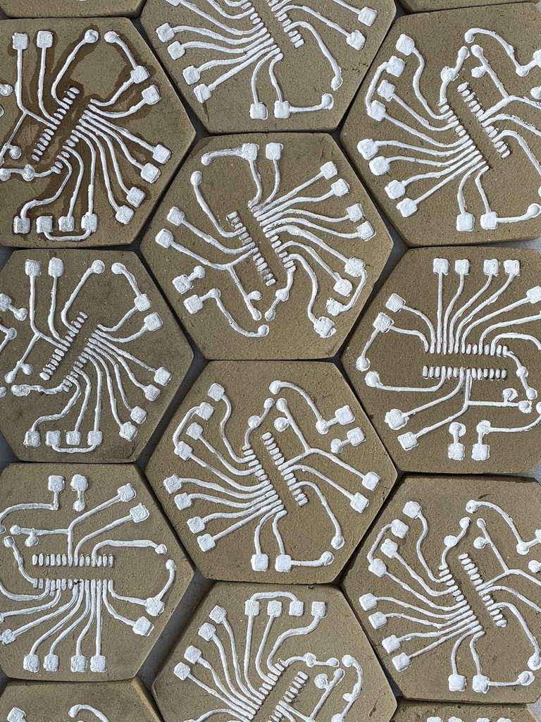
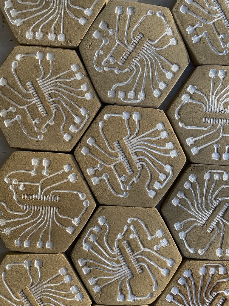
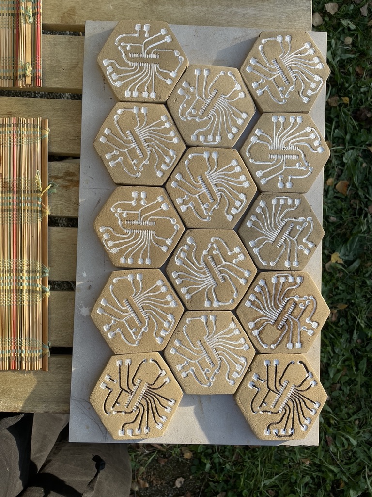
You will know when a board is 100% dry when you see its colour becoming lighter and more even. When it is not completely dry, although the edges turn a lighter colour, in the middle the clay is darker and wet. Our experience tells us that this is the minimum drying period required before starting to paint the circuits. If you wish, you can facilitate the painting process by gently sanding the boards, using a 120# or finer sanding paper. After sanding, make sure there is no dust on the board so you can start painting it.
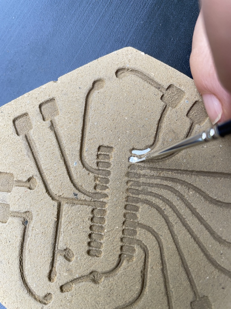
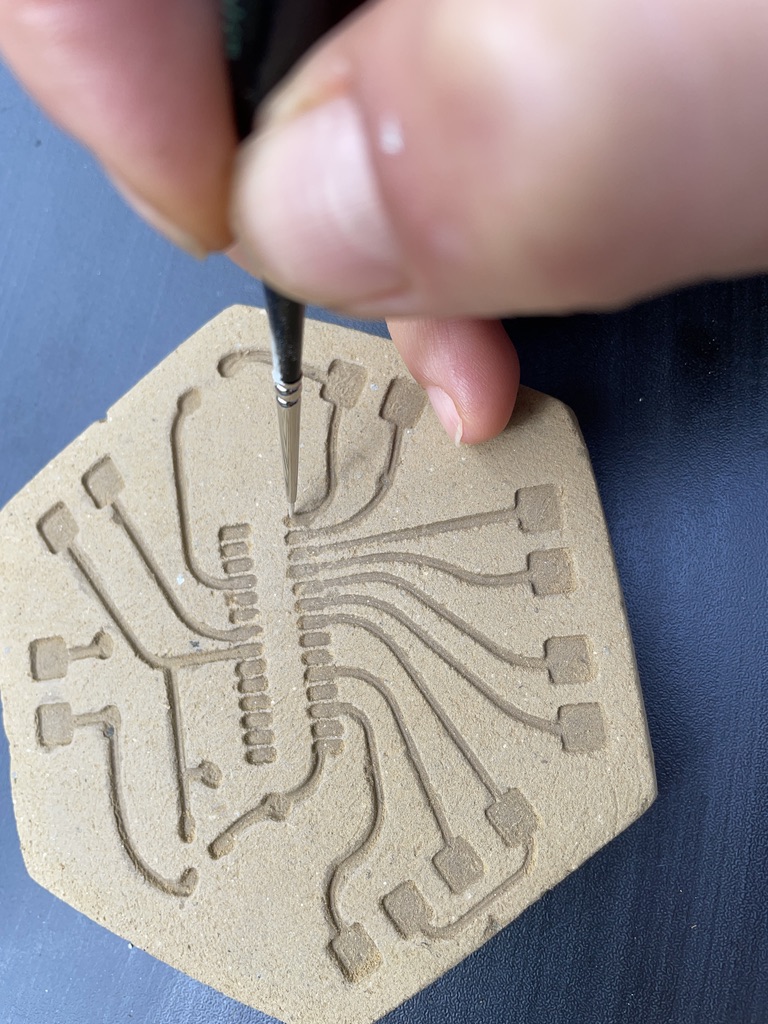
Painting the circuit
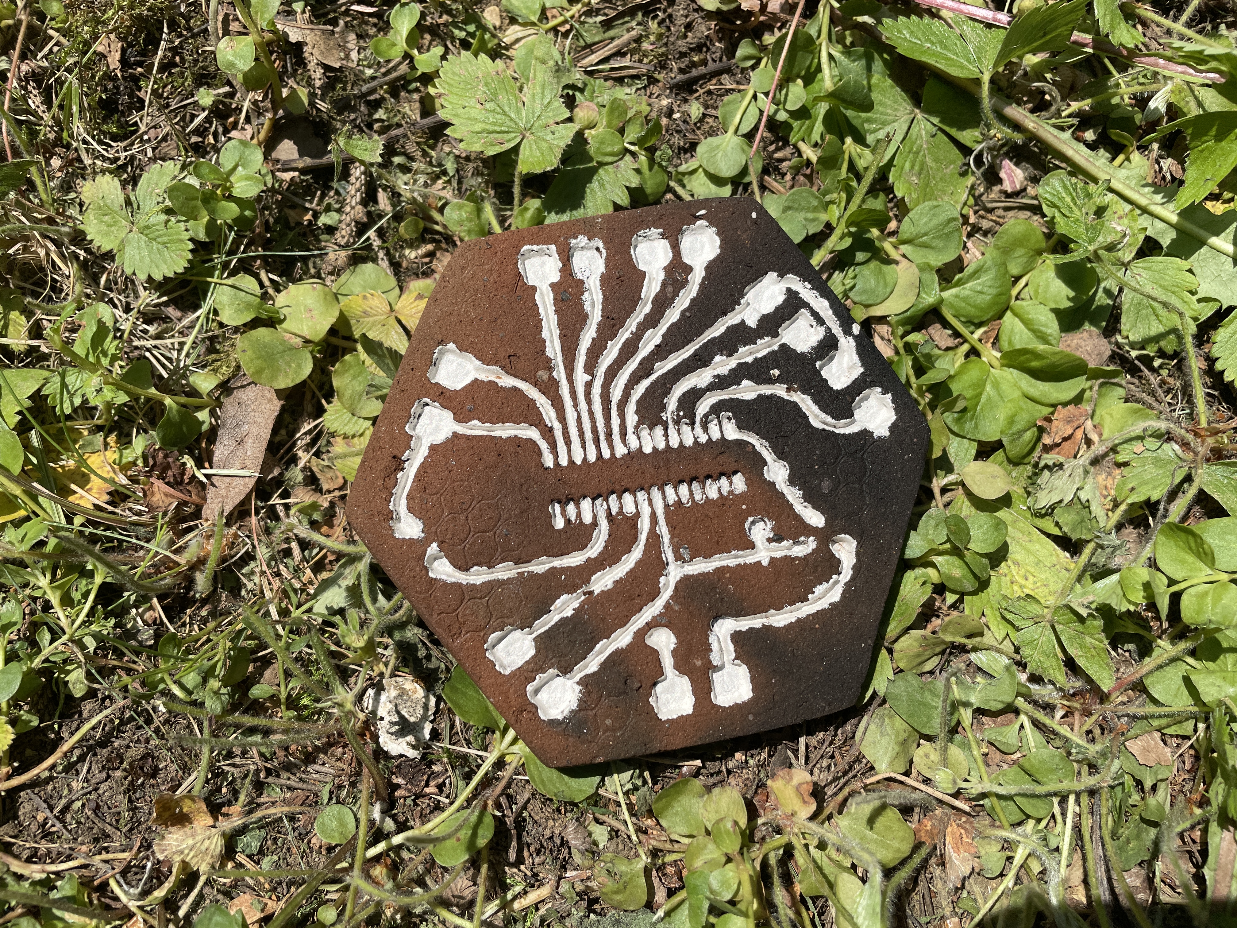
While searching for conductive materials that can be used in ceramics, we came across a gold lustre (used often for the gold details on porcelain) that, after firing, becomes conductive. The first problem we encountered was that this product is usually sold by ceramic shops that don"t supply any information about its ingredients, especially on the sources of the gold and its commodity chain. The second problem is that it is not possible to solder directly on this gold lustre, so we had to add another precious metal to the equation. The challenge was finding – within the solderable and easily available precious metals, such as tin, copper, brass and silver – one that could bear the firing process, which is c. 700 oC, and at the same time maintain its conductive properties. As we know, tin, which is mostly used for soldering, melts at a very low temperature, copper melts at approximately 1000 oC, but the oxidation process happens so quickly in the fire that it loses its conductive properties, and the same happens with brass. We were left with silver, which, although it also oxidises with the fire, maintains its conductive properties. Also, silver is cheaper than gold and widely used by goldsmiths. We were able to find a silver paint, commercialised by a German company, that is made with waste silver powder collected by jewellery makers. It's like an urban mining technique of silver dust.
While searching for conductive materials that can be used in ceramics, we came across a gold lustre (used often for the gold details on porcelain) that, after firing, becomes conductive. The first problem we encountered was that this product is usually sold by ceramic shops that don"t supply any information about its ingredients, especially on the sources of the gold and its commodity chain. The second problem is that it is not possible to solder directly on this gold lustre, so we had to add another precious metal to the equation. The challenge was finding – within the solderable and easily available precious metals, such as tin, copper, brass and silver – one that could bear the firing process, which is c. 700 oC, and at the same time maintain its conductive properties. As we know, tin, which is mostly used for soldering, melts at a very low temperature, copper melts at approximately 1000 oC, but the oxidation process happens so quickly in the fire that it loses its conductive properties, and the same happens with brass. We were left with silver, which, although it also oxidises with the fire, maintains its conductive properties. Also, silver is cheaper than gold and widely used by goldsmiths. We were able to find a silver paint, commercialised by a German company, that is made with waste silver powder collected by jewellery makers. It's like an urban mining technique of silver dust.
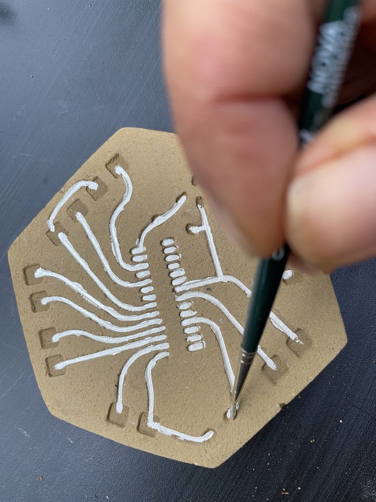
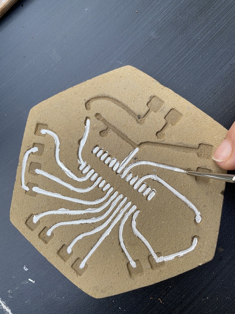
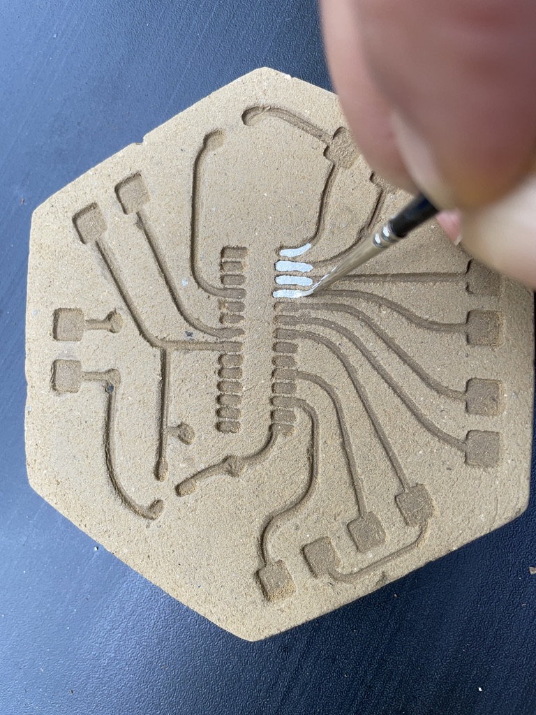
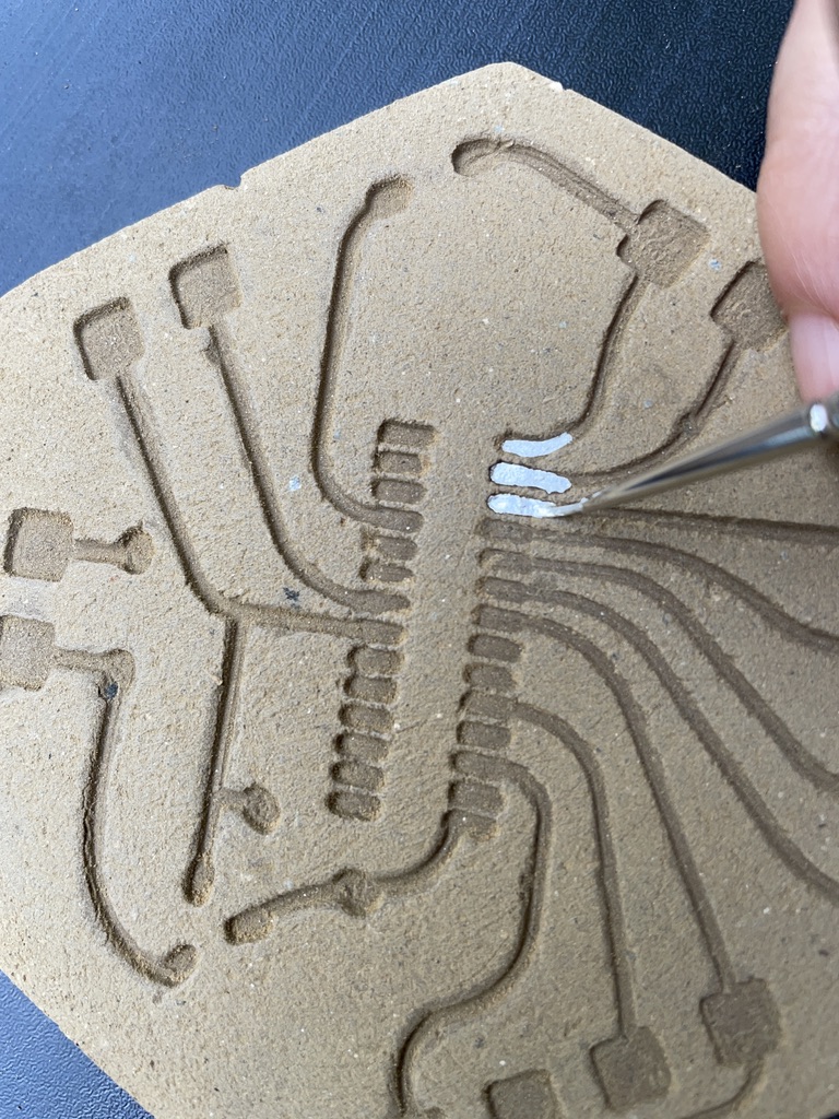
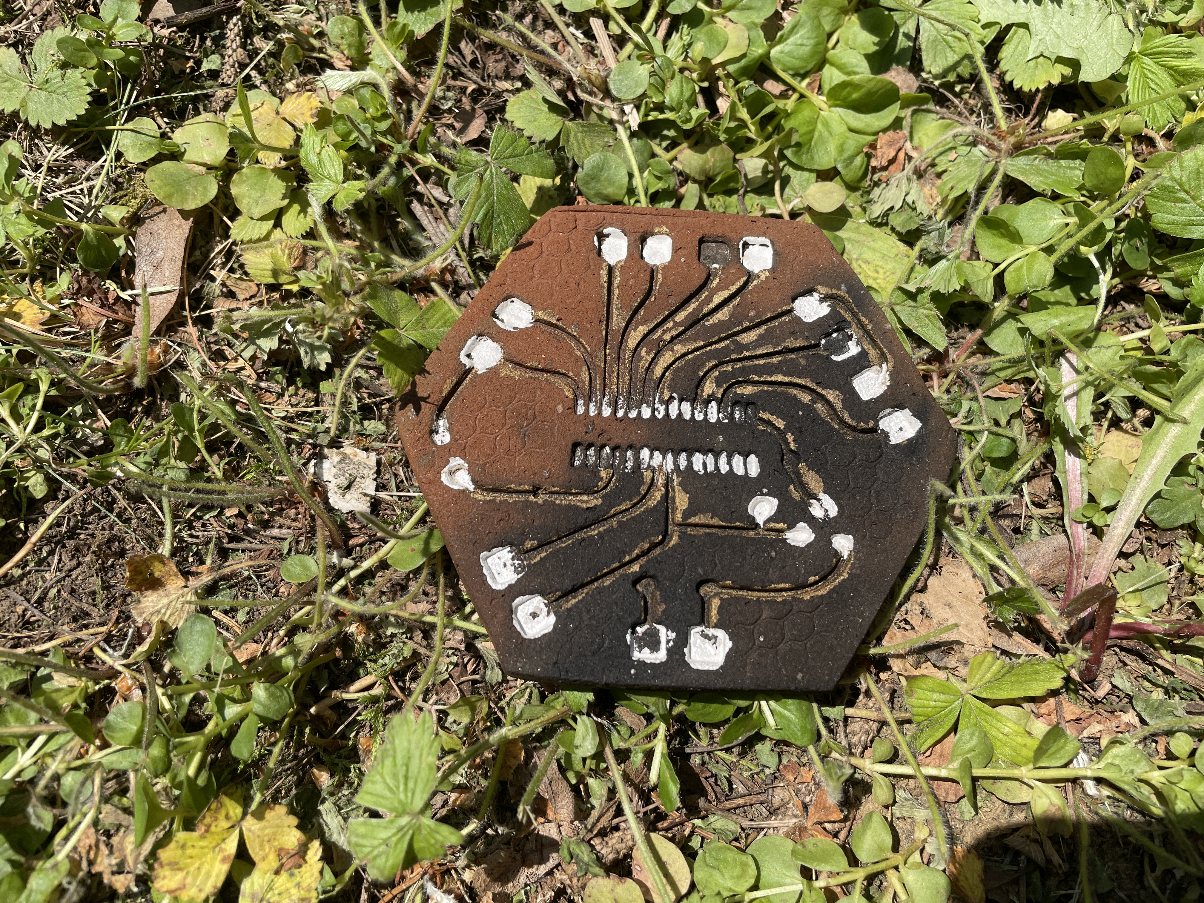
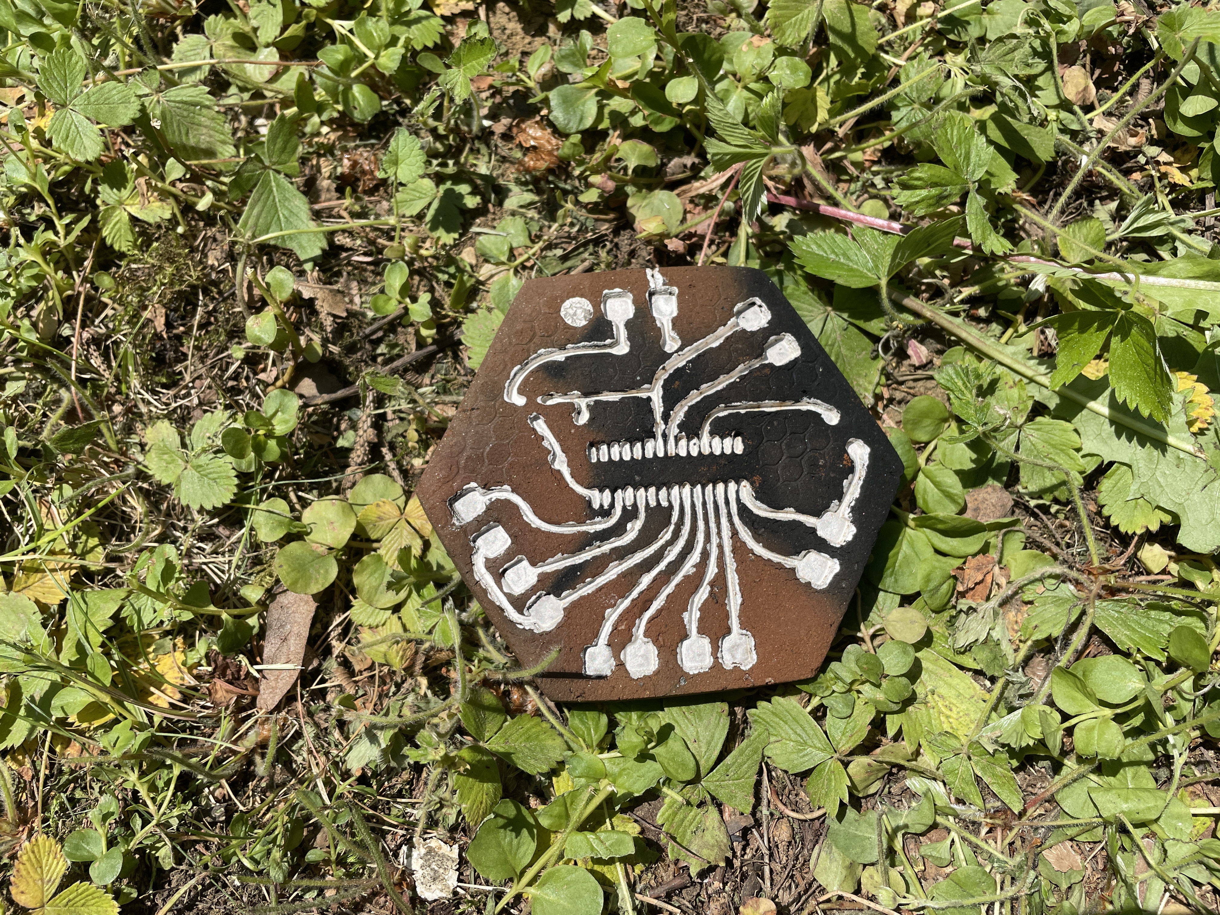
To paint the circuit, you will need a very thin brush, size 0/5. We recommend starting
from the middle, at the place where the ATmega chip will be soldered. These, and the
input and output connector pins, are the ones to which you should apply more silver
paint. It is important that the lines of silver do not touch one another. If that happens
(and it always does), you can correct it using a thin metal piece and scratching it out.
For the input and output connector pins, since the paintable area is larger, we used a
thicker brush (0 or 1).
There would have been many other ways to print the circuit without the time- consuming hand painting, for instance using a stencil mask and either spraying on it or using another paint-transferring technique. The reason we chose this method is because it appears to be more economical and sustainable, since you generate almost no waste paint.
There would have been many other ways to print the circuit without the time- consuming hand painting, for instance using a stencil mask and either spraying on it or using another paint-transferring technique. The reason we chose this method is because it appears to be more economical and sustainable, since you generate almost no waste paint.
Firing
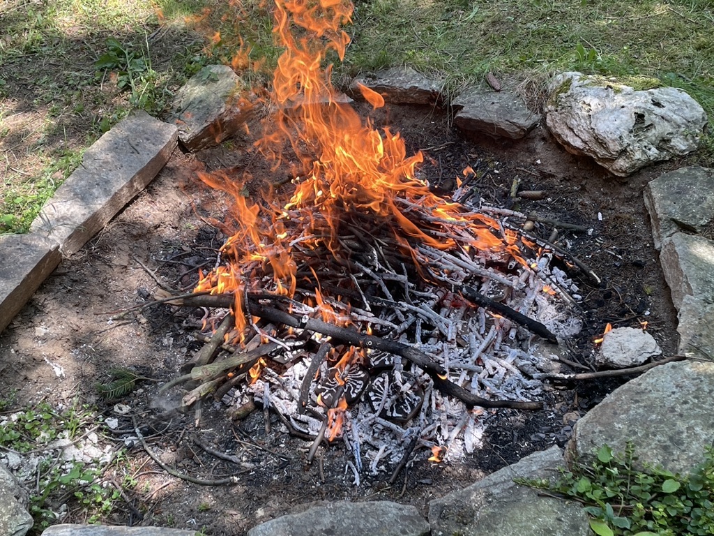
We fired the boards in our own backyard, reusing a hole that had been dug specifically for the purpose. The wood was collected in situ, consisting of dry wood sticks and old branches from our trees. We started a normal fire to generate some heat and placed all the boards around it to complete the drying process. Meanwhile, we collected wood sticks of approximately the same size but in two categories of thickness. The thicker sticks can be used for the base of the boards and the thinner ones can go on top.
We fired the boards in our own backyard, reusing a hole that had been dug specifically for the purpose. The wood was collected in situ, consisting of dry wood sticks and old branches from our trees. We started a normal fire to generate some heat and placed all the boards around it to complete the drying process. Meanwhile, we collected wood sticks of approximately the same size but in two categories of thickness. The thicker sticks can be used for the base of the boards and the thinner ones can go on top.
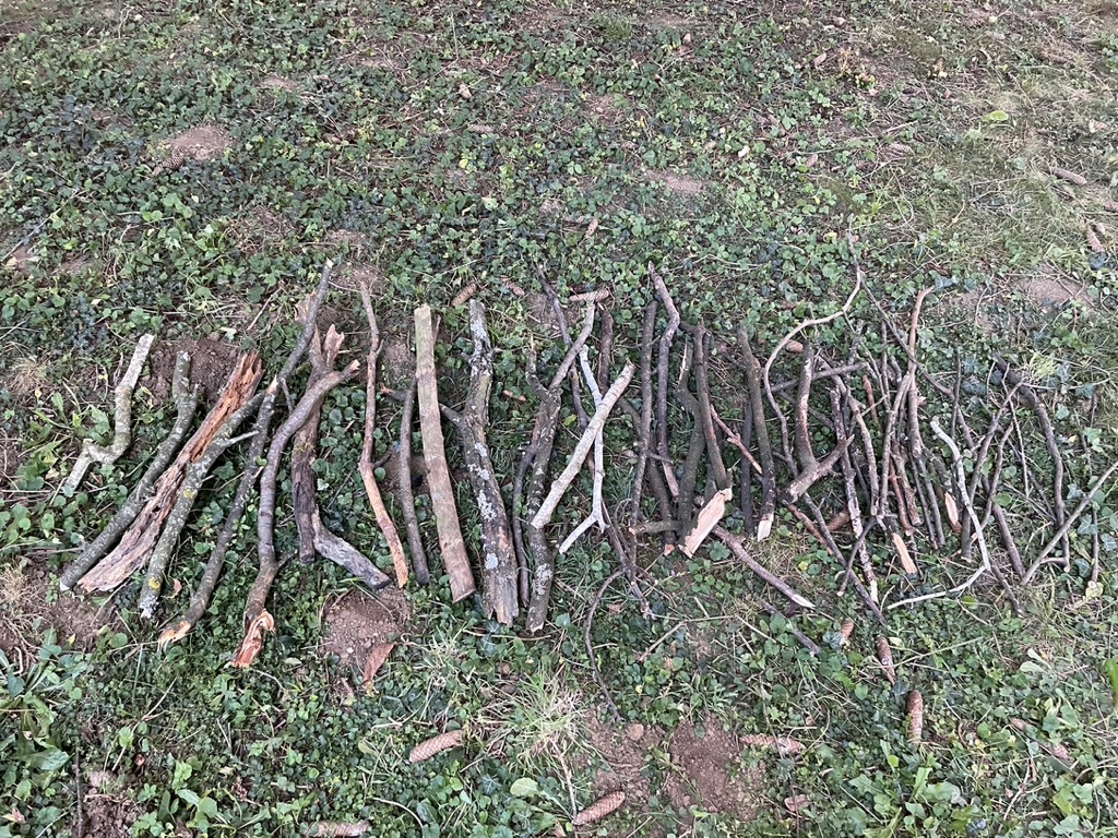
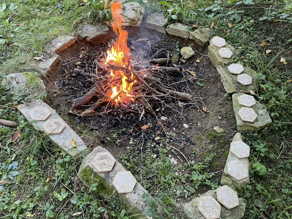
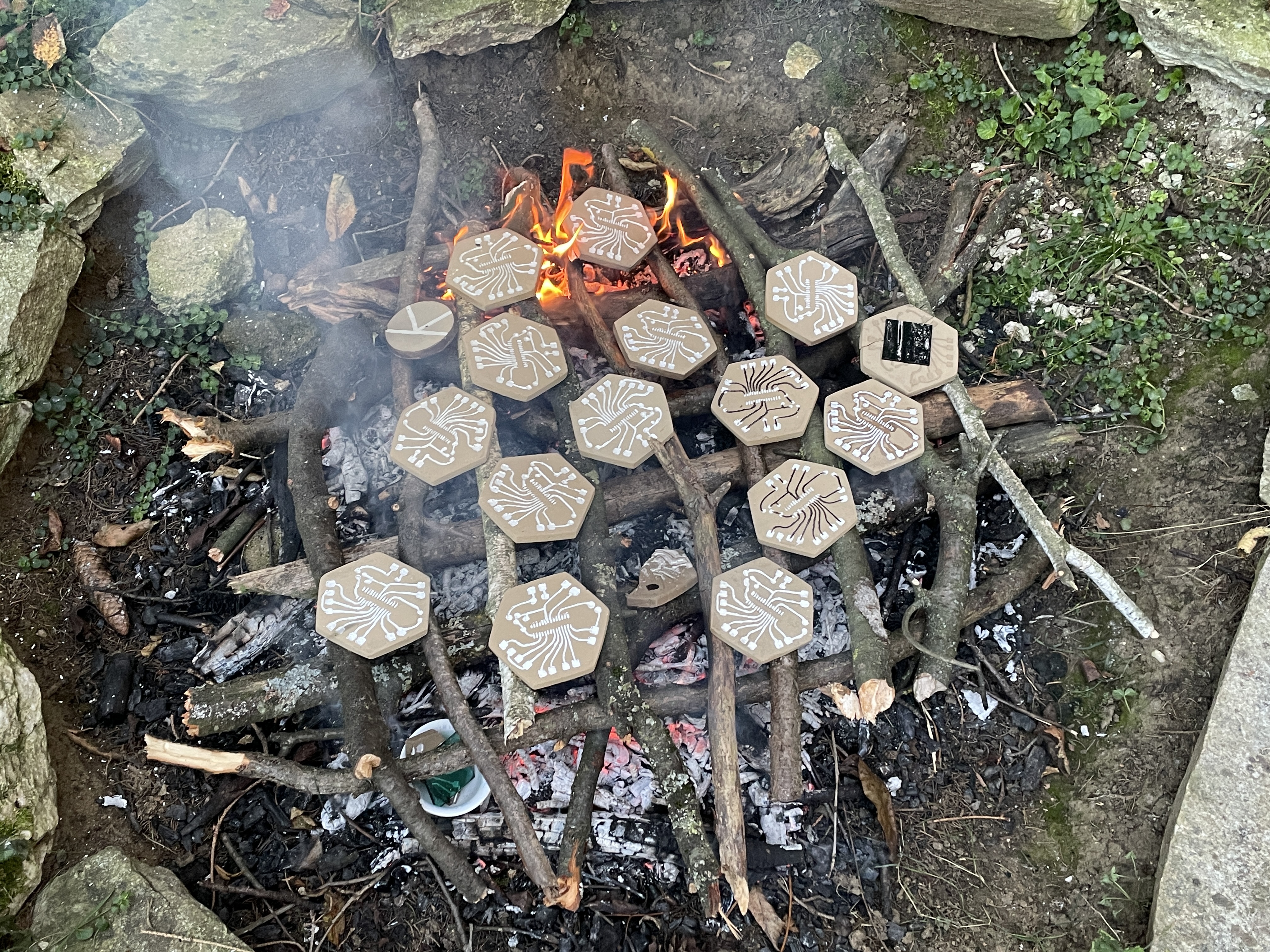

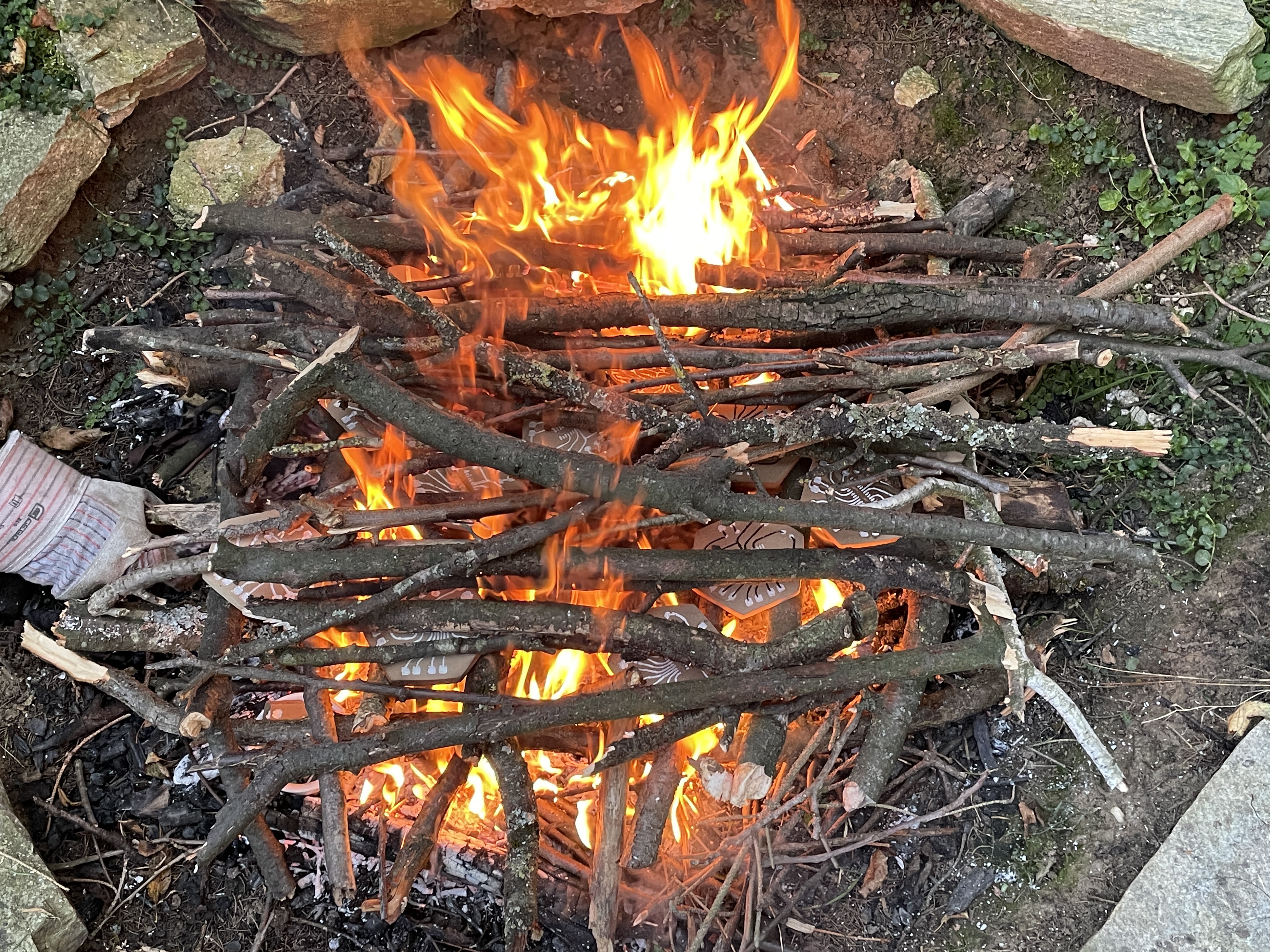
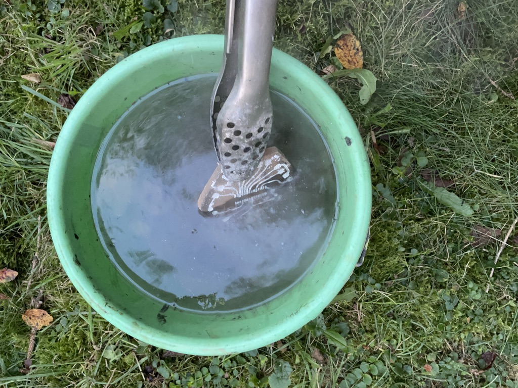
While the first fire is settling, you can start to build the !bed’ for the boards by placing
the first layer in parallel and the second transversely on top. Using proper fire-proof
gloves, glasses and clothes, start to add the boards to the top of the !bed’/ rack. We
used BBQ tongs to handle the boards.
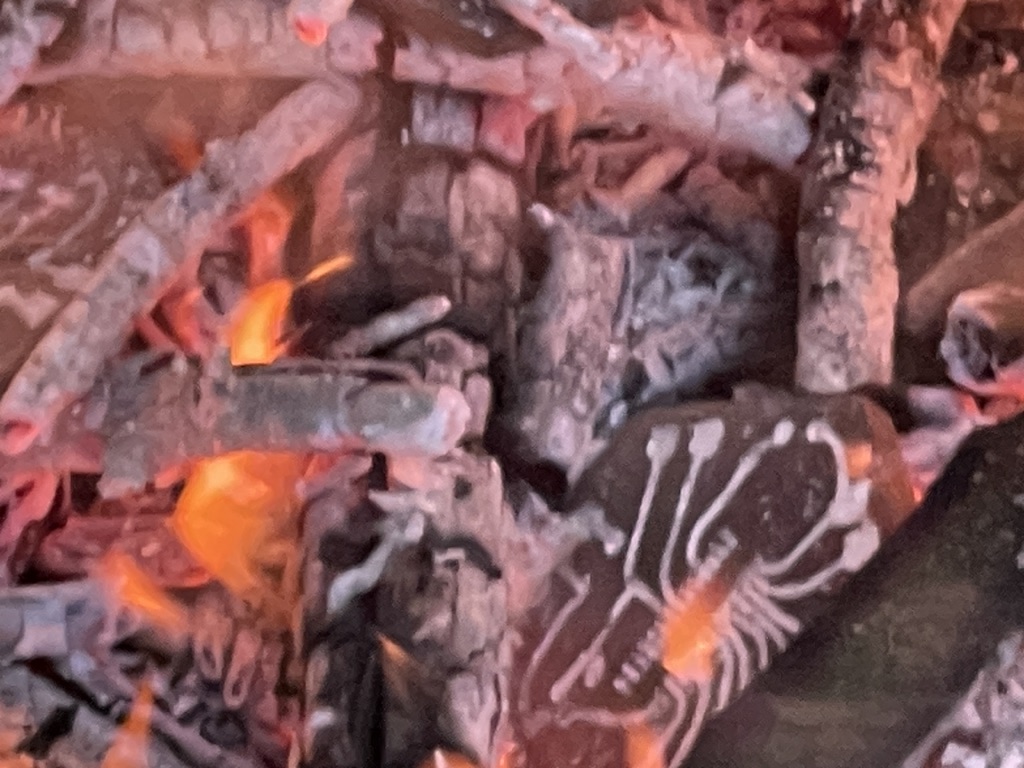
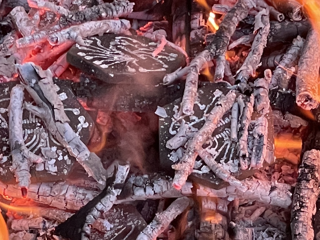
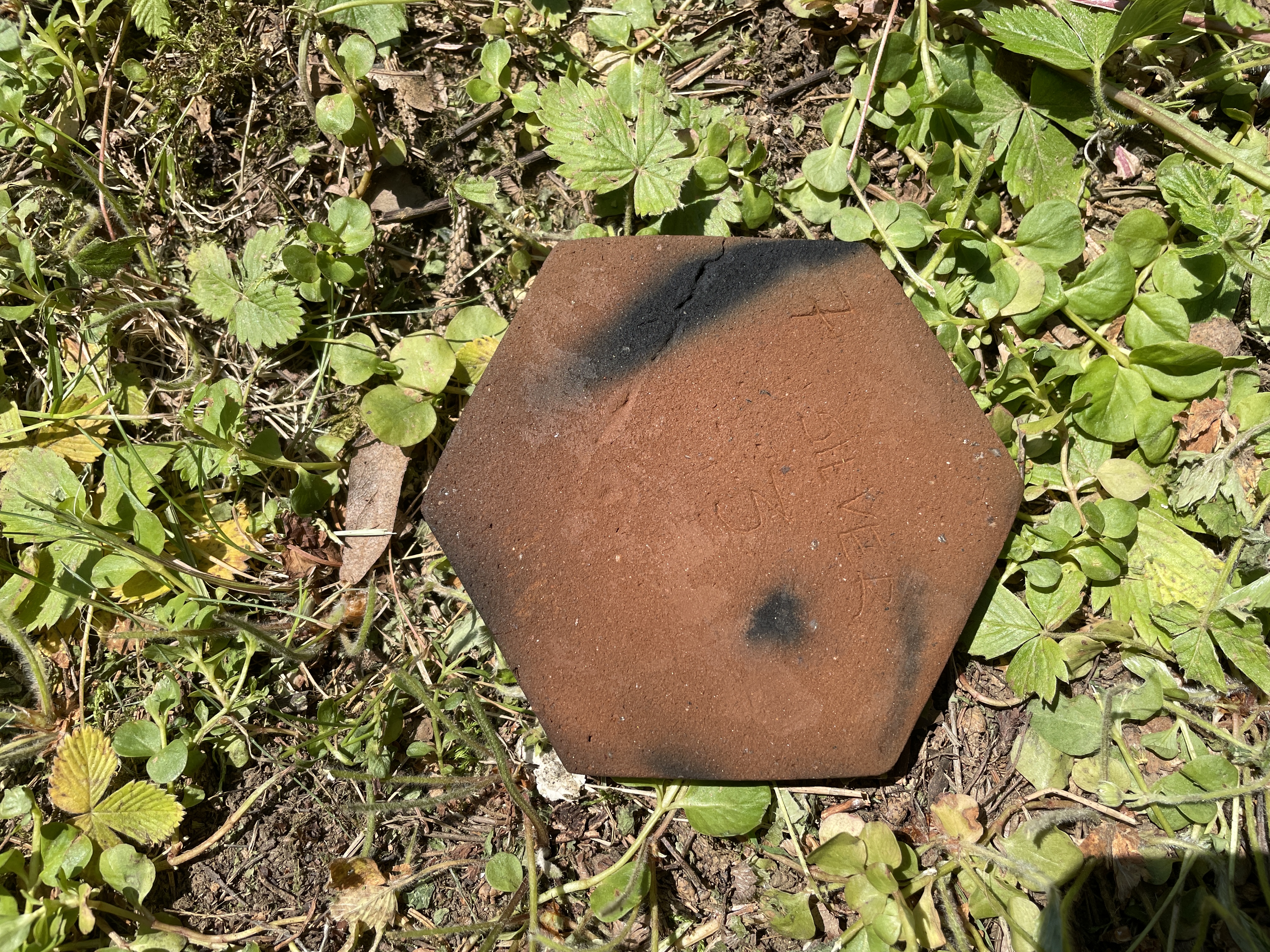
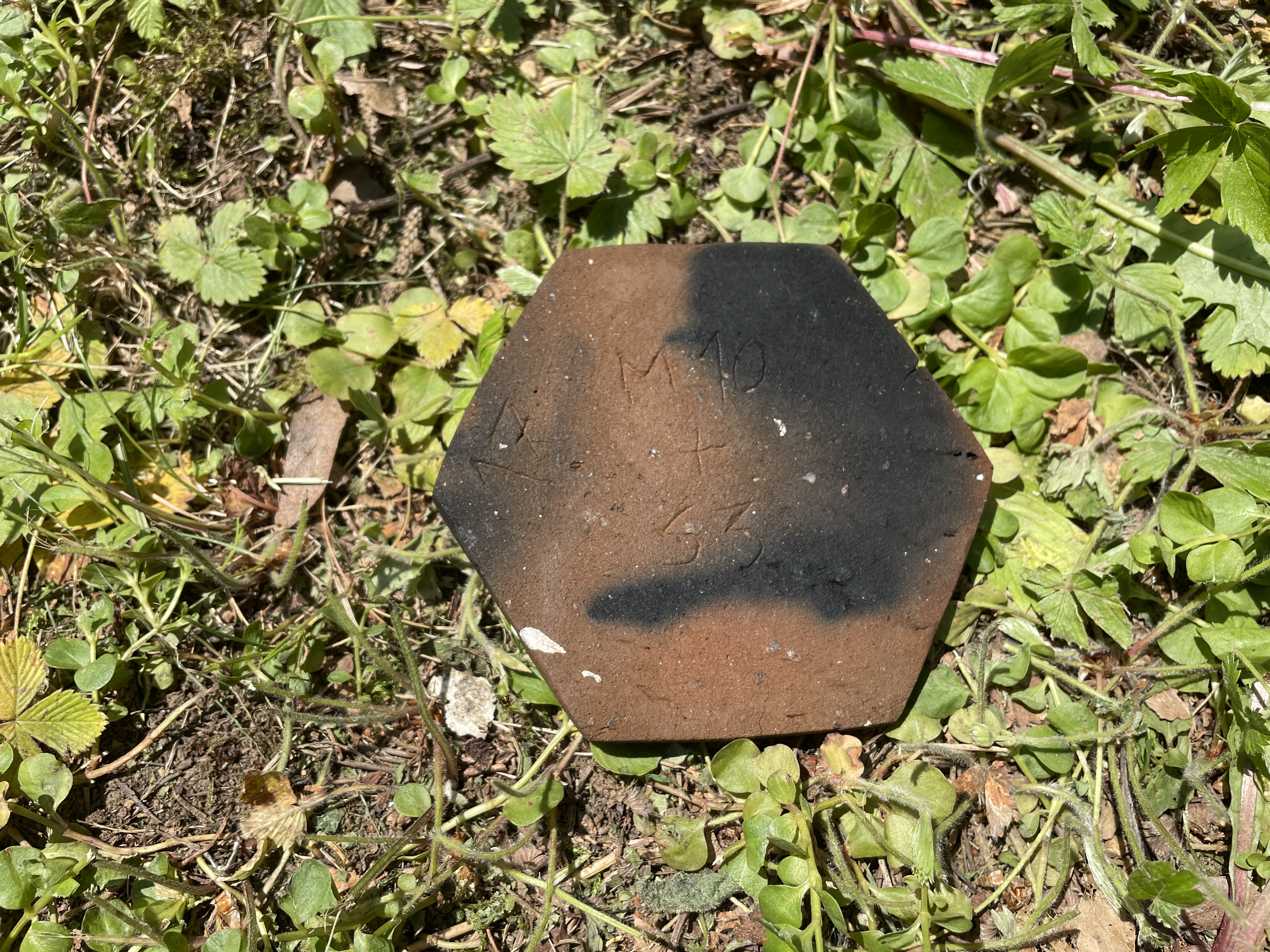
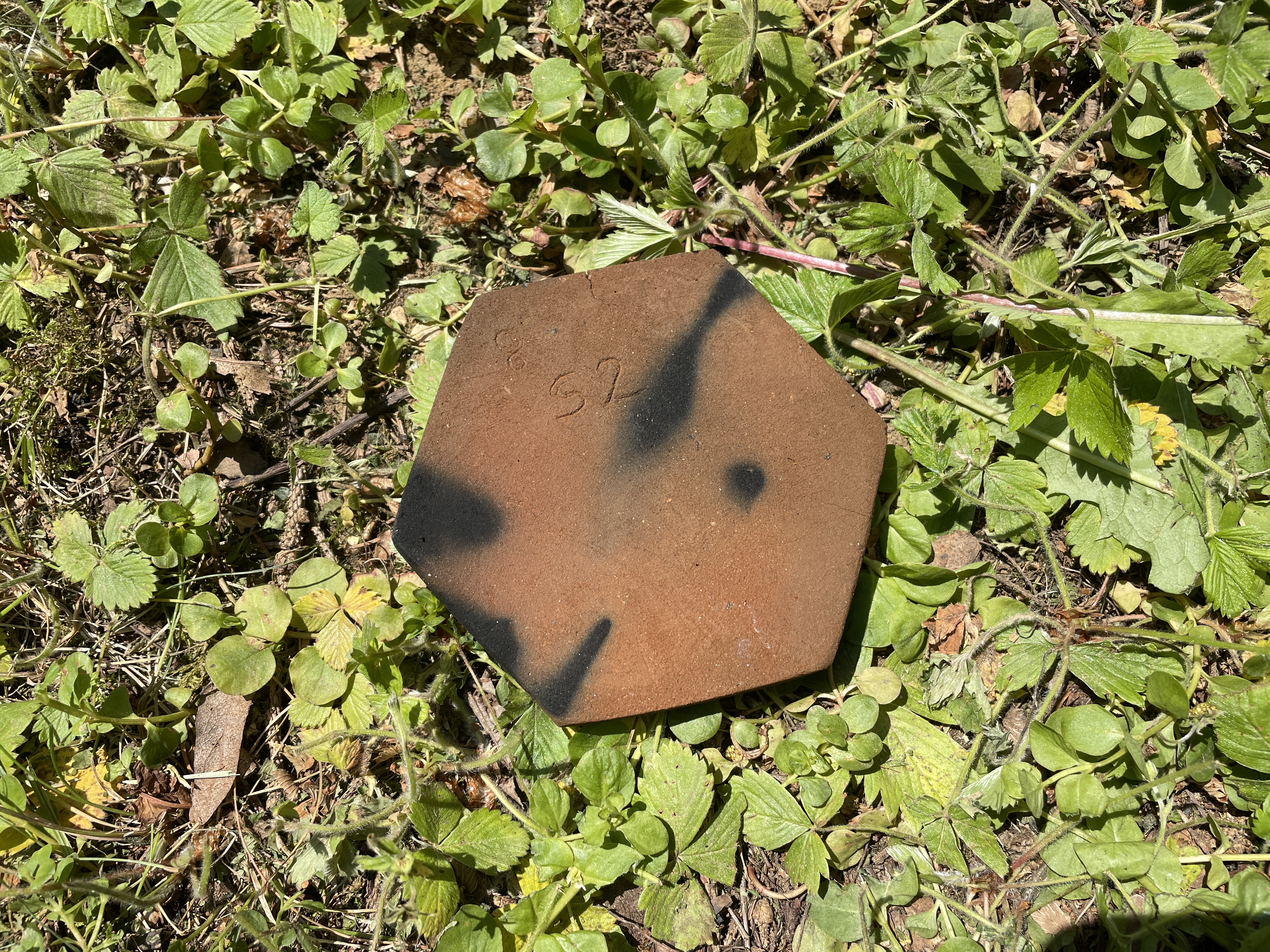
Quickly add the second layer by repeating the same process, only now with thinner sticks. This will cause the fire to expand and also provide an oven effect for the ceramic pieces. The maximum temperature should be around 700 oC, bearing in mind that it can be hard to control. Our experience tells us that 20 minutes is the average time they need to be ready, so you will need to keep the fire alive during that time. After 20 minutes, you can let the fire go down and check the boards. You should be able to see them glow in the fire, which is when you will know they are ready. Using the tongs, you can quickly transfer them from the fire to a bucket of cold water and leave them there, still holding them with the tongs for a few seconds. This is usually the ultimate !proof’ test for the clay. If there are no air bubbles, stones or cracks, and it has dried properly, it can resist the cold water.
Quickly add the second layer by repeating the same process, only now with thinner sticks. This will cause the fire to expand and also provide an oven effect for the ceramic pieces. The maximum temperature should be around 700 oC, bearing in mind that it can be hard to control. Our experience tells us that 20 minutes is the average time they need to be ready, so you will need to keep the fire alive during that time. After 20 minutes, you can let the fire go down and check the boards. You should be able to see them glow in the fire, which is when you will know they are ready. Using the tongs, you can quickly transfer them from the fire to a bucket of cold water and leave them there, still holding them with the tongs for a few seconds. This is usually the ultimate !proof’ test for the clay. If there are no air bubbles, stones or cracks, and it has dried properly, it can resist the cold water.
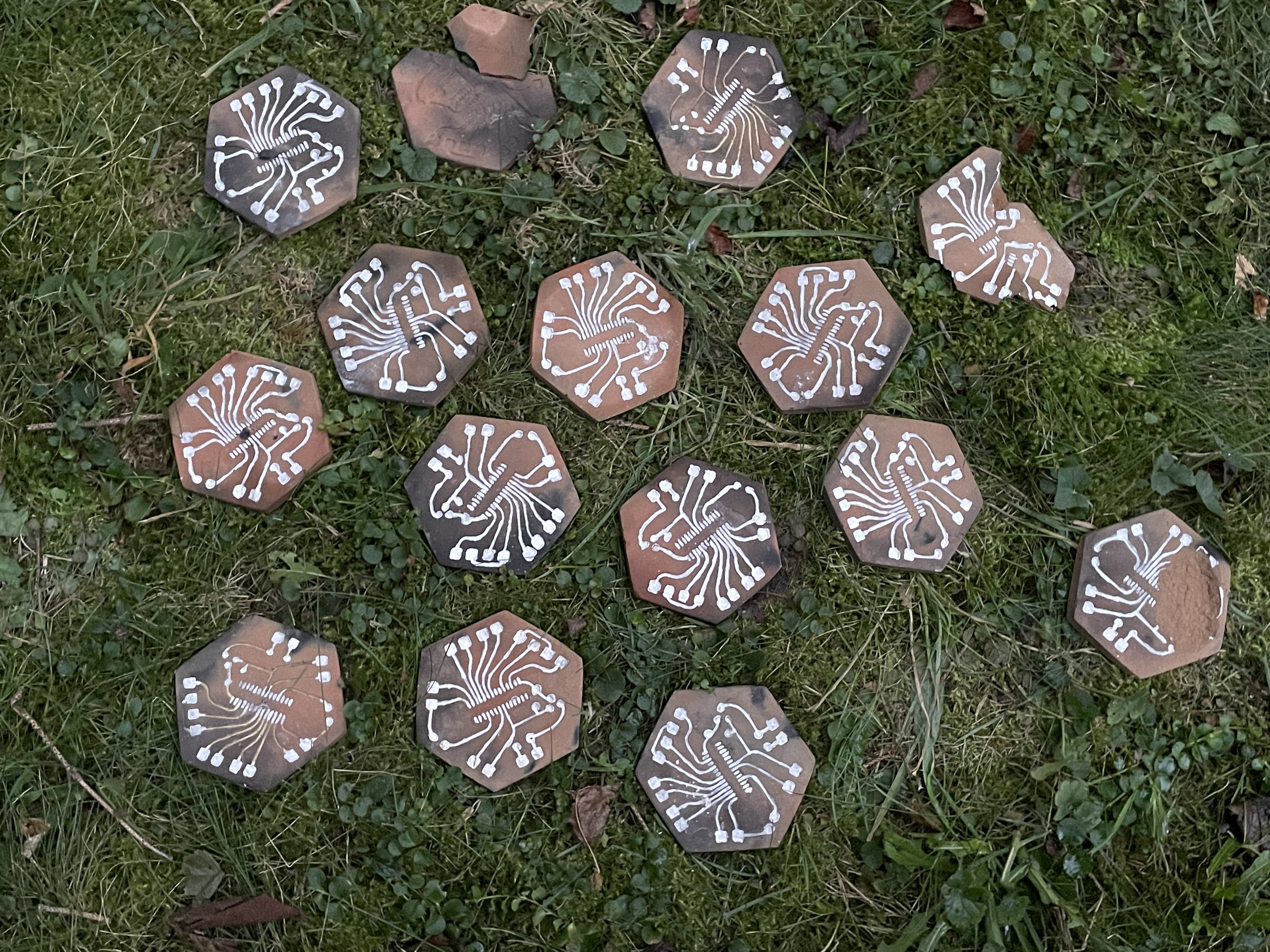
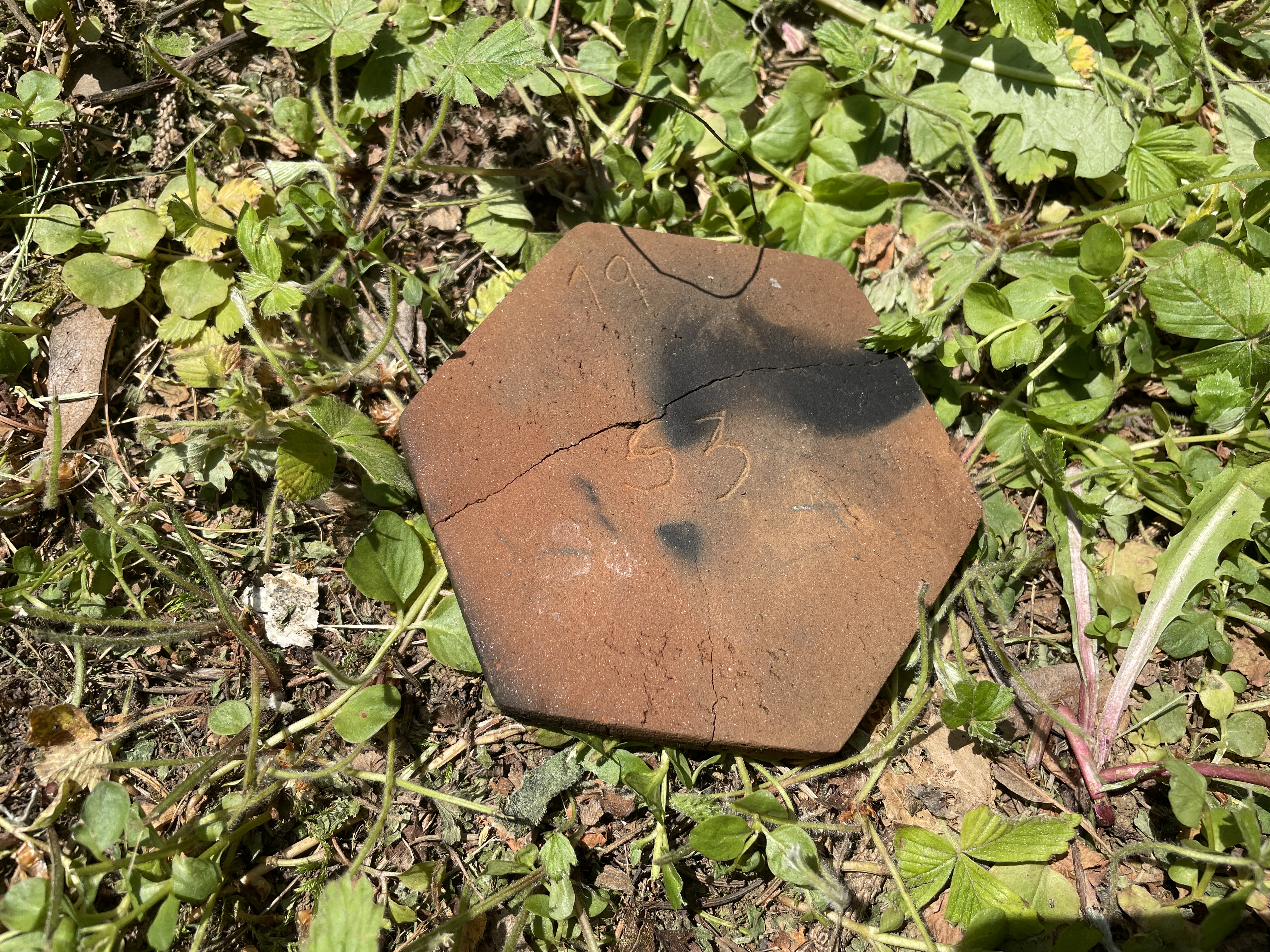
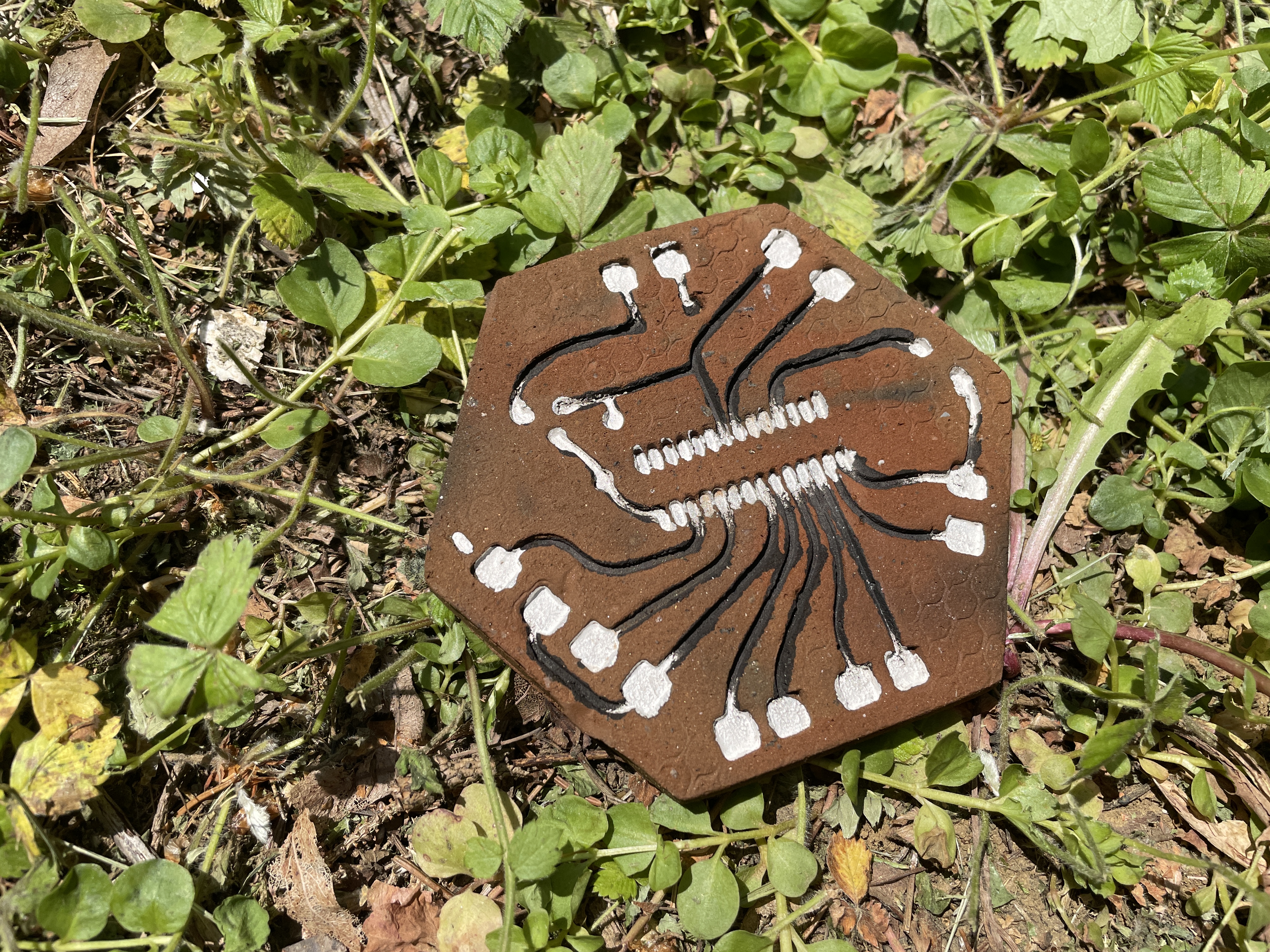
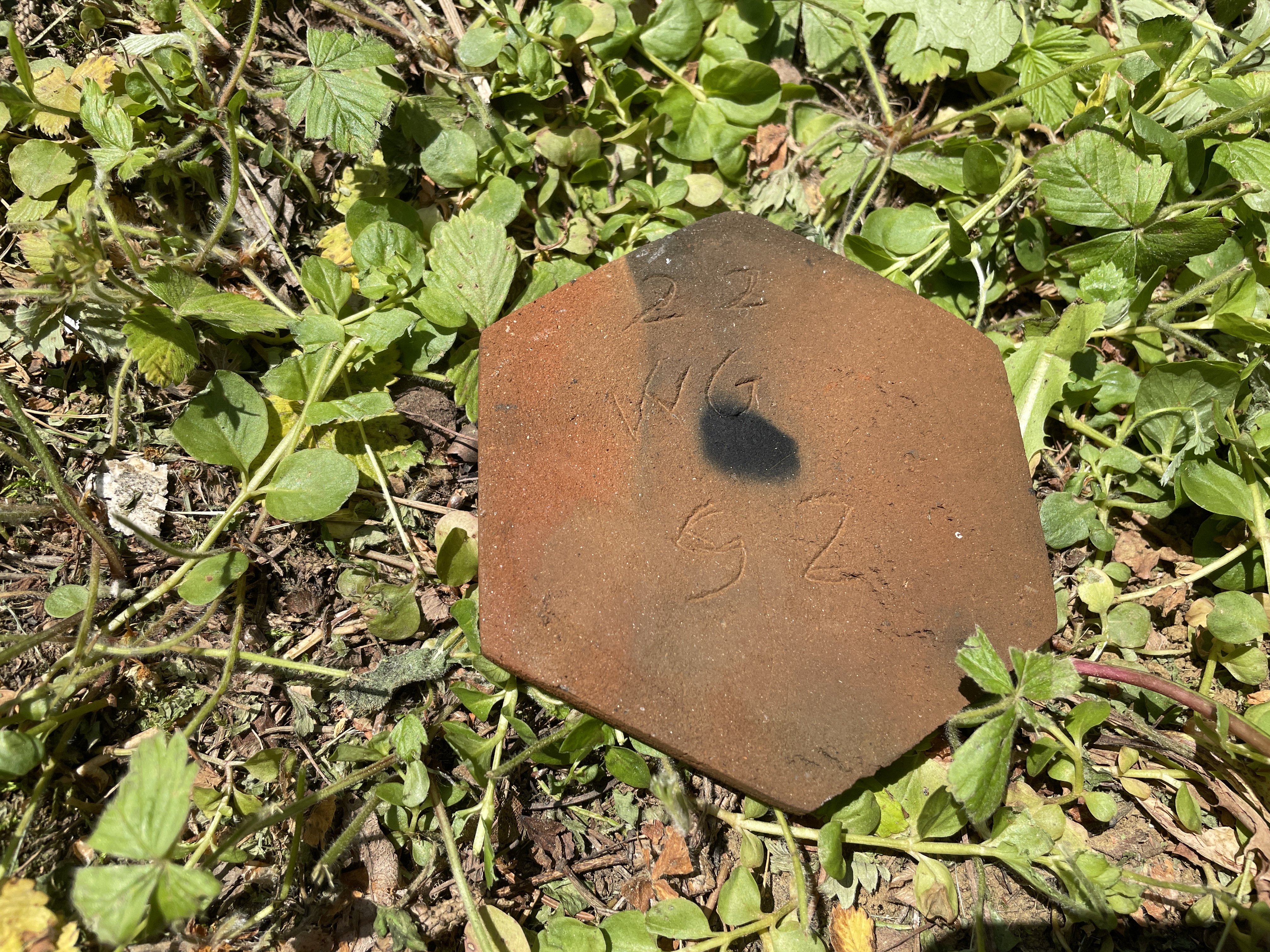
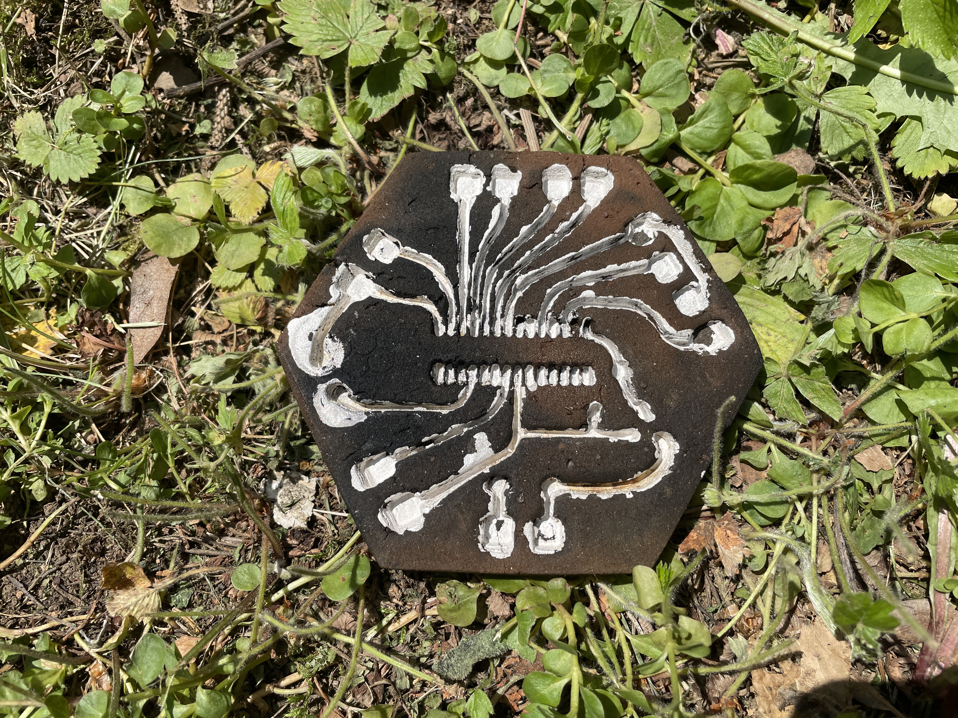
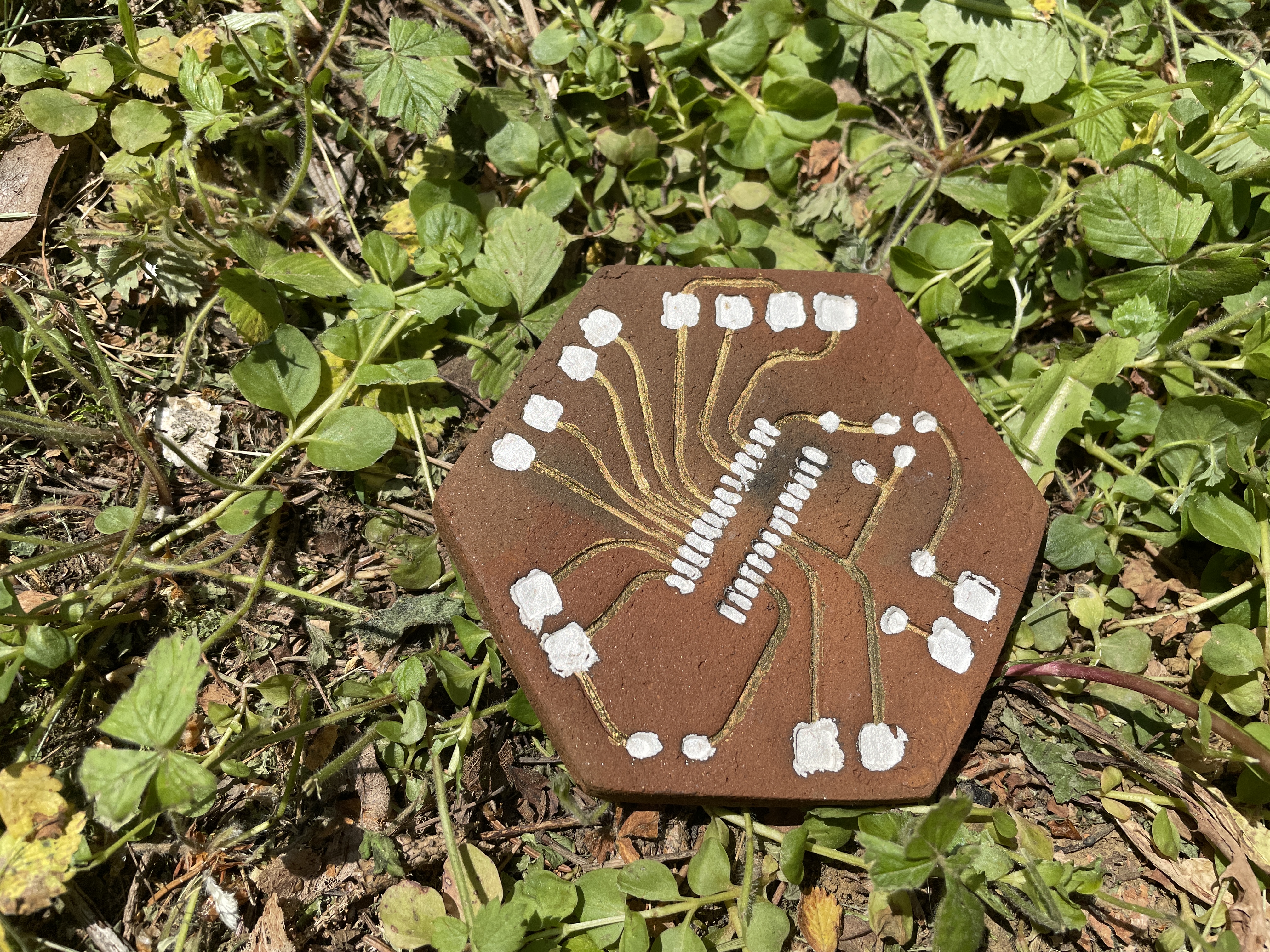
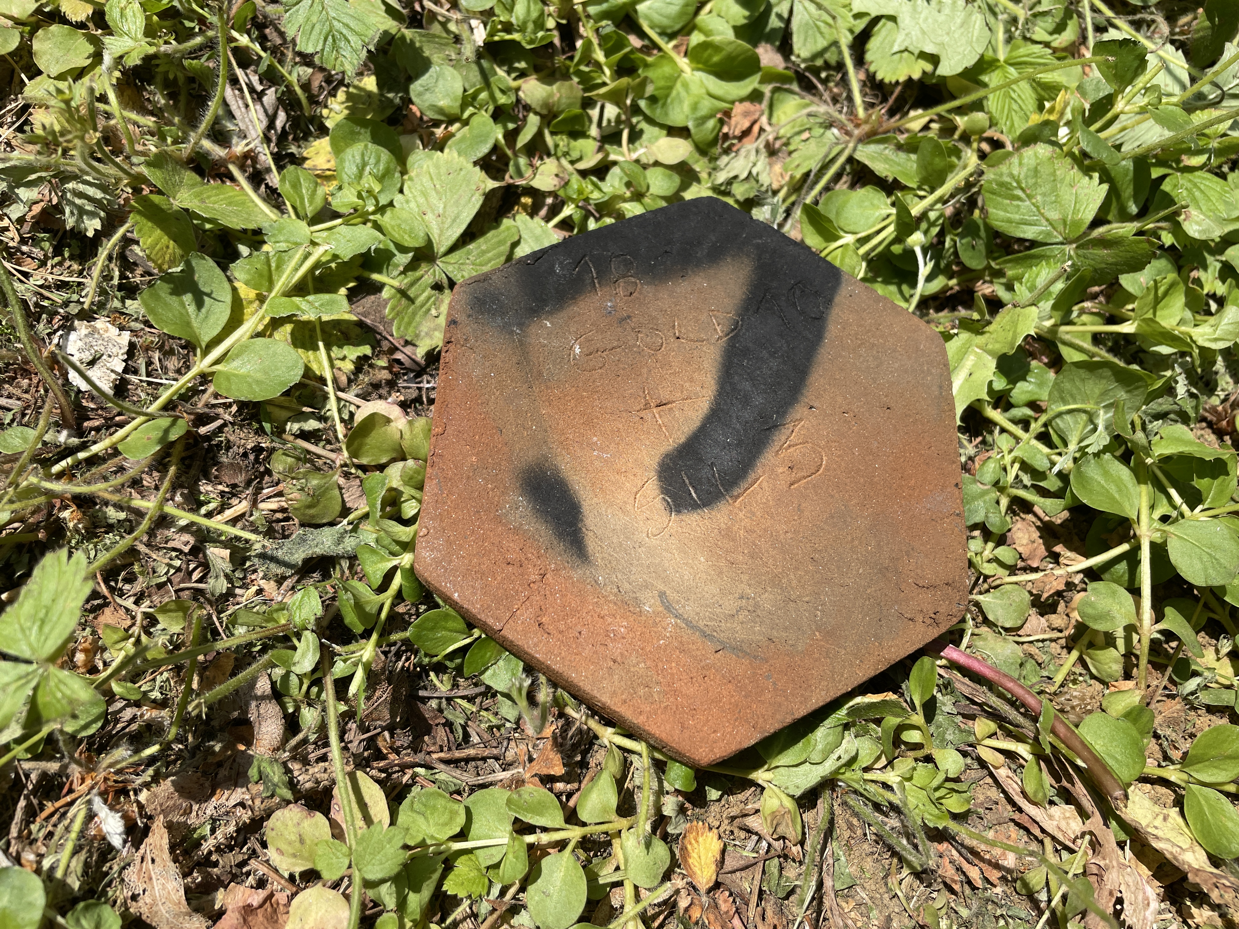
Our project is totally open sourced and you can find further instructions for Programming and soldering the components, 3D printing files, code in our GitHub https://github.com/FeministHardware/Making-PCBs-from-natural-clay
Credits:
Concept and Design: Patrícia J. Reis & Stefanie Wuschitz
PCB Design: Patrícia J. Reis & Daniel Schatzmayr
3D Printing: Klemens Kohlweis
Clay research: Patrícia J. Reis
Concept and Design: Patrícia J. Reis & Stefanie Wuschitz
PCB Design: Patrícia J. Reis & Daniel Schatzmayr
3D Printing: Klemens Kohlweis
Clay research: Patrícia J. Reis
