#eye #eye


Clay PCB


MaKING Printed Circuit Boards with Natural Clay


It is an open secret that the hardware in our smart devices contains not only plastics but also conflict minerals such as tungsten, tin, tantalum, silver and gold.

We are investigating alternative hardware from locally sourced materials, so-called ethical hardware, to develop and speculate upon renewable practices for the benefit of both nature and humans.


We are exploring different materials, sentient, low-impact, non-toxic, fair traded, recycled and urban mined means of production.

We aim to challenge the common PCB (printed circuit board) economies in an artistic, creative, positive and responsible way applying feminist hacking as an artistic methodology and critical framework.


Our initial idea was to develop a microcontroller PCB that could work with the chip ATmega328P, commonly used in the famous Arduino Uno board (or Arduina board how some feminists call it). Why this chip? Because we are part of community Hackerspace — Mz* Baltazar’s Lab (a feminist hacklab and artist run off-space based in Vienna, Austria)— and the Arduino Uno has been our favorite microcontroller in the past 12 years. After using it in many prototypes, artworks, workshops, we had many malfunction Arduino boards left. But it turned out that their chips were actually still working. The idea was to re-use these chips in our new project.

The second thought and challenge was to come up with an electric circuit that would allow us to receive several forms of input signal (analog and digital sensors) and generate a variety of output signal (to control leds, motors and speakers).

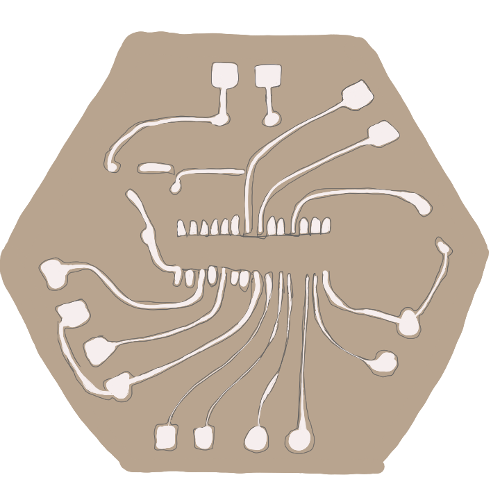
With this insight we were able to design a 3D printed “Stamp” using recycled Polypropylene filament. This process took a while, because it had to take into consideration the clay’s changed size after drying and firing. All clay is shrinking in size considerably during the drying and firing process. We come up with 5% shrinking percentage, but this number might vary depending on the clay you work with. We also made some experiments with the deepness of the circuit tracks and realized that ideally the imprint should be 1.2 mm deep.
To build the base of our PCB we needed insulating, sustainable and robust materials (maybe eggshells? Wood plates? wax? Ceramics?). We immediately went for ceramics, in particular porcelain, as it already plays an important role in electronic components such as capacitors, Piezo, resistors, etc... Porcelain is an industrial made material composed by Kaolin (the main ingredient that makes it plastic and white) and Stone Pottery (the second ingredient that makes porcelain translucent and hard). Both are well known commodities prospected and mined around the world, in small scale in Europe and bigger scale in China, Brazil, South Africa, Vietnam (among others).

In pottery, Porcelain, also known as China Clay, is a very delicate and sensitive material, (we could say it comes with its own agency), more difficult to control if compared with other industrial clays. Also, along with the other harder and resistant stoneware clays it usually requires higher firing temperatures in two Stages: a first firing known as ceramic bisque of c.a. 1000o C and a Glazing firing around 1200o C in an electric Kiln. During our first experiments with Porcelain we were immediately aware that those higher temperatures and therefore electric consumptions were not compatible with our standards for Ethical Hardware.
It was exactly when we struggled with the question of how to manufacture clay in low energy and low impact ways, that we came across the work of Heinz Lackinger. Heinz Lackinger is a pottery crafter in Donnerskirchen, Burgenland in Austria that works with prehistoric techniques of firing clay in an open wood fire. Instead of sophisticated machines, he only uses a simple hole in the ground of his 18th century backyard house. We had the privilege of spending two days with this skilled craftsman, learning how to identify and collect the clay, how to model it and fire it just using old, dry branches collected from forest ground. If the clay is collected in awareness of its many qualities and in small quantities only, this process can be defined as 100% fair trade and congruent with locally sourced modes of hardware production. We owe the knowledge required for the following steps to Heinz Lackinger’s generous knowledge transfer during his workshop and our own experiments with later applying this technique in the making of Natural Clay PCB boards.

We collected our clay in the beginning of fall in dry weather. The soil is mainly dry but does not consist only in argil: you will find little stones, plants, and even small insects. When the clay is that dry, the easiest way to clean it is by using a net that retains the undesirable waste. Our favorite tool is a normal kitchen colander. The waste collected should be given back to earth, back into the ground.


You will end up with a fine powder that will require some added water. We calculated an average of 100 ml of water per 1 kg of fine powder. Mixing it is just like blending flour and water, but without the inconvenient grumps. You should end up with something like a ball of clay after 10 minutes of massage. It is important that the clay sticks together and that all the air is out.


For the shape of our PCB board we used a hexagon tile cutter with 10 x 10 cm that can be purchased in common ceramic shops. The hexagon shape, as the tile form is not mandatory; you can do any shape and pick any thickness you desire, as long as it maintains a printable surface of c.a. 10 x 10 cm. We choose this shape and format in hope of assembling the boards as tiles next to each other, connecting them electronically. In the end we abandoned this idea since it was very difficult with this material, to obtain straight edges that could exactly meet each other sidewise.

To facilitate the process, we used two small wooden slats with 1 cm thickness, attached with clamps on a table. The distance between the slats is c.a. 10 cm. We also used a newspaper sheet underneath to avoid, that the clay sticks to the surface of the table. (Ideally a plaster surface works better.) Before placing the clay between the slats it is important to prepare it in small quantities. Each board requires around 180 gr so we recommend to take something around 220 gr and knead it thoroughly for a minute to get rid of air bubbles, to form it in the shape of a ball. (If your clay is not homogenous enough, better to throw it down forcefully against a flat surface and repeat the process a couple of times). When you’re ready, place it in between the slates and gently press it bearing down on it until it is flattened enough for the area you would like to achieve. We used a dough roller to flatten out the clay to 1 cm of thickness.

You will notice that the clay is very fragile and not as elastic as the industrial type. It will tend to break on the edges, which is fine, as long as that part is out of your inner cutter area.

After cutting out the hexagon with the hexagon tile cutter you can now place the stamp gently on the clay, facing down the 3D printed side towards the clay. It is important to apply some force but only quite gently, until the circuit is imprinted in the clay. In this process you force the clay to deform a little on the edges, but you can easily get rid of that excess material by sanding it after drying.


We usually let the boards dry naturally and outdoors for 24 hours before painting, but this time-frame is weather dependent. If you have got more time between modeling and firing the clay, you would ideally dry them indoors for one to two weeks, positioned between wooden plates and while applying some weight on the top plate. In this way they will not deform while drying and will maintain their flat surfaces. (We recommend using newspaper between the boards and the wood). If you want to dry them quickly you can also place them around a wood fire. It is important to avoid temperature clashes during drying so the best is to bring them to the fire as slowly as possible step by step.

You will know when a board is 100% dry when you see its color becoming lighter and more homogeneous. When it is not completely dry the edges become lighter color whereas in the middle the clay is still darker and wet. In any case, our experience tells us that this is the minimum drying period required to start to paint the circuits. If you wish, you can facilitate the painting process, by gently sanding the boards, using a 120 or finer sanding paper. After sanding, make sure all the dust is out of the board, so you can start with painting.


Painting the circuit

While searching for conductive materials that can be used in ceramics we came across a gold lustre (used often in gold details on porcelain) that after firing becomes conductive. The first problem we encountered was that this product is usually sold by ceramic shops that don’t supply any information on its ingredients, especially no information on the sources of the gold and its commodity chain. The second problem was the fact that it is not possible to solder directly on this gold lustre, so we needed to add another precious metal to the equation.

The challenge was to find within the solderable and easily available precious metals, such as tin, copper, brass and silver, one that could bear with the firing process which is c.a. 700o C and at the same time keep its conductive properties. As we know tin, mostly used for soldering, melts at a very low temperature, copper melts at approx. 1000C, but the oxidation process happens so quickly in the fire that it loses its conductive properties, the same happens with brass. We were left with silver, which although it also oxides with the fire, it keeps its conductive properties. Also silver is a cheaper metal than gold and is widely used by goldsmiths. We were able to find a silver paint commercialized by a German company that is made with waste silver powder collected by jewelry makers. It's kind of an urban mining technique of silver dust.
For painting the circuit you will need a very thin brush, size 0/5. We recommend starting from the middle at the place where the Atmega chip will be soldered. These and the input and output connector pins are the ones to which you should apply more silver paint. Important in this process is that the lines of silver do not touch each other. If that happens (which always does) you can correct it by using a thin metal piece and scratch it out. For the input and output connector pins, since the paintable area is bigger, we used a thicker brush (0 or 1).

There would have been many other ways to print the circuit avoiding that time consuming hand painting, as for instance using a stencil mask and either spray on it or use another paint transferring technique. The reason we choose this one is because it appears to be more economical and sustainable since you generate almost no waste paint.
Firing

We fired the boards in our private backyard, re-using a hole that was previously dug for that purpose. The wood was collected in-situ and it consists basically of dry wood sticks and old branches from our trees. We started a normal fire to gain some heat and placed all the boards around it so they can complete their drying process. In the meanwhile, we collected wood sticks with approx. the same size but in two thickness categories. The ticker sticks can be used for the base of the boards and the thinner to add on top.


While the first fire is lowering, you can start to build the “bed” for the boards by placing the first layer in parallel and the second transversely on top. Using proper fire- proof gloves, glasses, and clothes, start to add the boards on top of the “bed”/ rack. We used BBQ tongs to handle the boards.

Quickly add the second layer by repeating the same process, only now with thinner wood sticks. This will cause the fire to expand and also provide an oven effect for the ceramics pieces. The max temperature should be around 700C but that’s obviously hard to control. Our experience tells us that 20 minutes is the average time they need to be ready, so you will need to maintain the fire alive during that amount of time. After these 20 minutes you can let the fire get low by itself and check for the boards. You should be able to see them glow in the fire and that is the exact moment you will know that they are ready. Using the tongs you can now quickly transfer them from the fire to a cold water bucket and leave them there, yet still holding with the tongs for a few seconds. This is usually the ultimate “proof” test for the clay. If there were no air bubbles, stones or cracks, and if it dried properly, it can resist the cold water.
Our project is totally open sourced and you can find further instructions for Programming and soldering the components, 3D printing files, code in our GitHub https://github.com/FeministHardware/Making-PCBs-from-natural-clay
Here you can download the PDF with a full manual: 

Credits:

Concept and Design: Patrícia J. Reis & Stefanie Wuschitz

PCB Design: Patrícia J. Reis & Daniel Schatzmayr

3D Printing: Klemens Kohlweis

Clay research: Patrícia J. Reis